Thin slice of semiconductor used for the fabrication of integrated circuits
Top left: polished 12" and 6" silicon wafers. Their crystallographic orientation is marked by notches and flat cuts. Top right: VLSI microcircuits fabricated on a 12-inch (300mm) silicon wafer, before dicing and packaging.
Bottom left: A 3D rendering of solar wafers on a conveyor. Bottom right: completed solar wafers
In the semiconductor industry, the term wafer appeared in the 1950s to describe a thin round slice of semiconductor material, typically germanium or silicon. The round shape characteristic of these wafers comes from single-crystal ingots usually produced using the Czochralski method. Though, silicon wafers were first introduced in the 1940s.[2][3]
By 1960, silicon wafers were being manufactured in the U.S. by companies such as MEMC and SunEdison. In 1965, American engineers Eric O. Ernst, Donald J. Hurd, and Gerard Seeley, while working under IBM, filed Patent US3423629A[4] for the first high-capacity epitaxial apparatus.
Wafers are formed of highly pure,[5] nearly defect-free single crystalline material, with a purity of 99.9999999% (9N) or higher.[5] One process for forming crystalline wafers is known as the Czochralski method, invented by Polish chemist Jan Czochralski. In this process, a cylindrical ingot of high purity monocrystalline semiconductor, such as silicon or germanium, called a boule, is formed by pulling a seed crystal from a melt.[6][7] Donor impurity atoms, such as boron or phosphorus in the case of silicon, can be added to the molten intrinsic material in precise amounts in order to dope the crystal, thus changing it into an extrinsic semiconductor of n-type or p-type.
The boule is then sliced with a wafer saw (a type of wire saw), machined to improve flatness, chemically etched to remove crystal damage from machining steps and finally polished to form wafers.[8] The size of wafers for photovoltaics is 100–200mm square and the thickness is 100–500μm.[9] Electronics use wafer sizes from 100 to 450mm diameter. The largest wafers made have a diameter of 450mm,[10] but are not yet in general use.
Cleaning, texturing and etching
Wafers are cleaned with weak acids to remove unwanted particles. There are several standard cleaning procedures to make sure the surface of a silicon wafer contains no contamination. One of the most effective methods is the RCA clean. When used for solar cells, the wafers are textured to create a rough surface to increase surface area and so their efficiency. The generated PSG (phosphosilicate glass) is removed from the edge of the wafer in the etching.[11]
Wafer properties
Standard wafer sizes
Silicon substrate
Silicon wafers are available in a variety of diameters from 25.4mm (1inch) to 300mm (11.8inches).[12][13]Semiconductor fabrication plants, colloquially known as fabs, are defined by the diameter of wafers that they are tooled to produce. The diameter has gradually increased to improve throughput and reduce cost with the current state-of-the-art fab using 300 mm, with a proposal to adopt 450 mm.[14][15]Intel, TSMC, and Samsung were separately conducting research to the advent of 450 mm "prototype" (research) fabs, though serious hurdles remain.[16]
2-inch (51mm), 4-inch (100mm), 6-inch (150mm), and 8-inch (200mm) wafers
Wafers grown using materials other than silicon will have different thicknesses than a silicon wafer of the same diameter. Wafer thickness is determined by the mechanical strength of the material used; the wafer must be thick enough to support its own weight without cracking during handling. The tabulated thicknesses relate to when that process was introduced, and are not necessarily correct currently, for example the IBM BiCMOS7WL process is on 8-inch wafers, but these are only 200μm thick. The weight of the wafer increases with its thickness and the square of its diameter. Date of introduction does not indicate that factories will convert their equipment immediately, in fact, many factories do not bother upgrading. Instead, companies tend to expand and build whole new lines with newer technologies, leaving a large spectrum of technologies in use at the same time.
Gallium Nitride substrate
GaN substrate wafers typically have had their own independent timelines, parallel but far lagging silicon substrate, but ahead of other substrates. The world's first 300 mm wafer made of GaN was announced in Sept 2024 by Infineon, suggesting in the coming future they could put into use the first factory with 300 mm GaN commercial output.[20]
SiC substrate
Meanwhile world's first Silicon Carbide (SiC) 200 mm wafers were announced in July 2021 by ST Microelectronics.[21] It is not known if SiC 200 mm has entered volume production as of 2024, as typically the largest fabs for SiC in commercial production remain at 150 mm.
Silicon on sapphire
Silicon on sapphire (SOS) is a specific type of Silicon on Insulator (SOI) technology, where the insulating substrate is sapphire and the active superstrate is silicon. [22] Epitaxial layers and doping can be tailored as needed. SOS in commercial production is typically maxed out at 150 mm wafer sizes as of 2024.
Gallium Arsenide substrate
GaAs wafers tend to be 150 mm at largest, in commercial production as of 2024.[23]
Aluminum Nitride substrate
AlN tends to be 50 mm or 2 inch wafers in commercial production, while 100 mm or 4 inch wafers are being developed as of 2024 by wafer suppliers like Asahi Kasei. However, merely because a wafer exists commercially, does not imply in any way that processing equipment to produce chips on that wafer exists, indeed such equipment tends to lag development until paying end customer demand materializes. Even after equipment is developed (years), it can take further years for fabs to figure out how to use the machines productively.
Diamond substrate
Diamond tends to be 50-55 mm or ~2 inch wafers in prototype production, while commercial production is being targeted as of 2026.[24]
Historical increases of wafer size
A unit of wafer fabrication step, such as an etch step, can produce more chips proportional to the increase in wafer area, while the cost of the unit fabrication step goes up more slowly than the wafer area. This was the cost basis for increasing wafer size. Conversion to 300mm wafers from 200mm wafers began in early 2000, and reduced the price per die for about 30–40%.[citation needed]Larger diameter wafers allow for more die per wafer.
M1 wafer size (156.75mm) is in the process of being phased out in China as of 2020. Various nonstandard wafer sizes have arisen, so efforts to fully adopt the M10 standard (182mm) are ongoing. Like other semiconductor fabrication processes, driving down costs has been the main driving factor for this attempted size increase, in spite of the differences in the manufacturing processes of different types of devices.[citation needed]
Crystalline orientation
Diamond cubic crystal structure of a silicon unit cellFlats can be used to denote doping and crystallographic orientation. Red represents material that has been removed.
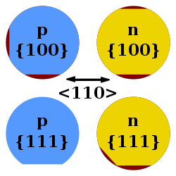
Wafers are grown from crystal having a regular crystal structure, with silicon having a diamond cubic structure with a lattice spacing of 5.430710 Å (0.5430710nm).[25] When cut into wafers, the surface is aligned in one of several relative directions known as crystal orientations. Orientation is defined by the Miller index with (100) or (111) faces being the most common for silicon.[25] Orientation is important since many of a single crystal's structural and electronic properties are highly anisotropic. Ion implantation depths depend on the wafer's crystal orientation, since each direction offers distinct paths for transport.[26]
Wafer cleavage typically occurs only in a few well-defined directions. Scoring the wafer along cleavage planes allows it to be easily diced into individual chips ("dies") so that the billions of individual circuit elements on an average wafer can be separated into many individual circuits.[citation needed]
Crystallographic orientation notches
Wafers under 200mm diameter have flats cut into one or more sides indicating the crystallographic planes of the wafer (usually a {110} face). In earlier-generation wafers a pair of flats at different angles additionally conveyed the doping type (see illustration for conventions). Wafers of 200mm diameter and above use a single small notch to convey wafer orientation, with no visual indication of doping type. 450 mm wafers are notchless, relying on a laser scribed structure on the wafer surface for orientation.[27]
Impurity doping
Silicon wafers are generally not 100% pure silicon, but are instead formed with an initial impurity doping concentration between 1013 and 1016 atoms per cm3 of boron, phosphorus, arsenic, or antimony which is added to the melt and defines the wafer as either bulk n-type or p-type.[28] However, compared with single-crystal silicon's atomic density of 5×10²² atoms per cm3, this still gives a purity greater than 99.9999%. The wafers can also be initially provided with some interstitial oxygen concentration. Carbon and metallic contamination are kept to a minimum.[29]Transition metals, in particular, must be kept below parts per billion concentrations for electronic applications.[30]
450 mm wafers
Challenges
There is considerable resistance to the 450mm transition despite the possible productivity improvement, because of concern about insufficient return on investment.[citation needed] There are also issues related to increased inter-die / edge-to-edge wafer variation and additional edge defects. 450mm wafers are expected to cost 4 times as much as 300mm wafers, and equipment costs are expected to rise by 20 to 50%.[31] Higher cost semiconductor fabrication equipment for larger wafers increases the cost of 450mm fabs (semiconductor fabrication facilities or factories). Lithographer Chris Mack claimed in 2012 that the overall price per die for 450mm wafers would be reduced by only 10–20% compared to 300mm wafers, because over 50% of total wafer processing costs are lithography-related. Converting to larger 450mm wafers would reduce price per die only for process operations such as etch where cost is related to wafer count, not wafer area.[citation needed] Cost for processes such as lithography is proportional to wafer area, and larger wafers would not reduce the lithography contribution to die cost.[32]
Nikon planned to deliver 450-mm lithography equipment in 2015, with volume production in 2017.[33][34] In November 2013 ASML paused development of 450-mm lithography equipment, citing uncertain timing of chipmaker demand.[35]
In 2012, a group consisting of New York State (SUNY Poly/College of Nanoscale Science and Engineering (CNSE)), Intel, TSMC, Samsung, IBM, Globalfoundries and Nikon companies has formed a public-private partnership called Global 450mm Consortium (G450C, similar to SEMATECH) who made a 5-year plan (expiring in 2016) to develop a "cost effective wafer fabrication infrastructure, equipment prototypes and tools to enable coordinated industry transition to 450mm wafer level".[36][37] In the mid of 2014 CNSE has announced that it will reveal first fully patterned 450mm wafers at SEMICON West.[38] In early 2017, the G450C began to dismantle its activities over 450mm wafer research due to undisclosed reasons.[39][40][41] Various sources have speculated that demise of the group came after charges of bid rigging made against Alain E. Kaloyeros, who at the time was a chief executive at the SUNY Poly.[41][40][42] The industry realization of the fact that the 300mm manufacturing optimization is more cheap than costly 450mm transition may also have played a role.[41]
The timeline for 450mm has not been fixed. In 2012, it was expected that 450mm production would start in 2017, which never realized.[43][44] Mark Durcan, then CEO of Micron Technology, said in February 2014 that he expects 450mm adoption to be delayed indefinitely or discontinued. "I am not convinced that 450mm will ever happen but, to the extent that it does, it's a long way out in the future. There is not a lot of necessity for Micron, at least over the next five years, to be spending a lot of money on 450mm."[45]
"There is a lot of investment that needs to go on in the equipment community to make that happen. And the value at the end of the day – so that customers would buy that equipment – I think is dubious."[46] As of March 2014, Intel Corporation expected 450mm deployment by 2020 (by the end of this decade).[47] Mark LaPedus of semiengineering.com reported in mid-2014 that chipmakers had delayed adoption of 450mm "for the foreseeable future." According to this report some observers expected 2018 to 2020, while G. Dan Hutcheson, chief executive of VLSI Research, didn't see 450mm fabs moving into production until 2020 to 2025.[48]
The step up to 300mm required major changes, with fully automated factories using 300mm wafers versus barely automated factories for the 200mm wafers, partly because a FOUP for 300mm wafers weighs about 7.5 kilograms[49] when loaded with 25 300mm wafers where a SMIF weighs about 4.8 kilograms[50][51][17] when loaded with 25 200mm wafers, thus requiring twice the amount of physical strength from factory workers, and increasing fatigue. 300mm FOUPs have handles so that they can be still be moved by hand. 450mm FOUPs weigh 45 kilograms[52] when loaded with 25 450mm wafers, thus cranes are necessary to manually handle the FOUPs[53] and handles are no longer present in the FOUP. FOUPs are moved around using material handling systems from Muratec or Daifuku. These major investments were undertaken in the economic downturn following the dot-com bubble, resulting in huge resistance to upgrading to 450mm by the original timeframe. On the ramp-up to 450mm, the crystal ingots will be 3 times heavier (total weight a metric ton) and take 2–4 times longer to cool, and the process time will be double.[citation needed] All told, the development of 450mm wafers requires significant engineering, time, and cost to overcome.
Analytical die count estimation
In order to minimize the cost per die, manufacturers wish to maximize the number of dies that can be made from a single wafer; dies always have a square or rectangular shape due to the constraint of wafer dicing. In general, this is a computationally complex problem with no analytical solution, dependent on both the area of the dies as well as their aspect ratio (square or rectangular) and other considerations such as the width of the scribeline or saw lane, and additional space occupied by alignment and test structures. (By simplifying the problem so that the scribeline and saw lane are both zero-width, the wafer is perfectly circular with no flats, and the dies have a square aspect ratio, we arrive at the Gauss Circle Problem, an unsolved open problem in mathematics.)
Note that formulas estimating the gross dies per wafer (DPW) account only for the number of complete dies that can fit on the wafer; gross DPW calculations do not account for yield loss among those complete dies due to defects or parametric issues.[citation needed]
Wafermap showing fully patterned dies, and partially patterned dies which don't fully lie within the wafer
the size of each die (mm2) including the width of the scribeline ( or in the case of a saw lane, the kerf plus a tolerance).
This formula simply states that the number of dies which can fit on the wafer cannot exceed the area of the wafer divided by the area of each individual die. It will always overestimate the true best-case gross DPW, since it includes the area of partially patterned dies which do not fully lie on the wafer surface (see figure). These partially patterned dies don't represent complete ICs, so they usually cannot be sold as functional parts.[citation needed]
Refinements of this simple formula typically add an edge correction, to account for partial dies on the edge, which in general will be more significant when the area of the die is large compared to the total area of the wafer. In the other limiting case (infinitesimally small dies or infinitely large wafers), the edge correction is negligible.[citation needed]
The correction factor or correction term generally takes one of the forms cited by De Vries:[54]
(area ratio – circumference/(die diagonal length))
or (area ratio scaled by an exponential factor)
or (area ratio scaled by a polynomial factor).
Studies comparing these analytical formulas to brute-force computational results show that the formulas can be made more accurate, over practical ranges of die sizes and aspect ratios, by adjusting the coefficients of the corrections to values above or below unity, and by replacing the linear die dimension with (average side length) in the case of dies with large aspect ratio:[54]
12SemiSource 2006: A supplement to Semiconductor International. December 2005. Reference Section: How to Make a Chip. Adapted from Design News. Reed Electronics Group.
↑LaPedus, Mark (January 14, 2009). "450-mm fab debate surfaces". EE Times. Aspencore. Retrieved 2021-05-09. As reported, Intel, TSMC and Samsung are separately pushing for the advent of 450-mm prototype fabs by 2012
↑"Nikon appointing head of precision equipment business as new president" (Press release). Japan: Nikon Corp. semiconportal. May 20, 2014. Nikon plans to introduce 450mm wafer lithography systems for volume production in 2017.
↑LaPedus, Mark (2013-09-13). "Litho Roadmap Remains Cloudy". semiengineering.com. Sperling Media Group LLC. Retrieved July 14, 2014. Nikon planned to ship 'early learning tools' by 2015. 'As we have said, we will be shipping to meet customer orders in 2015,' said Hamid Zarringhalam, executive vice president at Nikon Precision.
↑"ASML 2013 Annual Report Form (20-F)"(XBRL). United States Securities and Exchange Commission. February 11, 2014. In November 2013, following our customers' decision, ASML decided to pause the development of 450mm lithography systems until customer demand and the timing related to such demand is clear.
↑LaPedus, Mark (2014-05-15). "Is 450mm Dead In The Water?". semiengineering.com. California: Sperling Media Group LLC. Archived from the original on 2014-06-05. Retrieved 2014-06-04. Intel and the rest of the industry have delayed the shift to 450mm fabs for the foreseeable future, leaving many to ponder the following question—Is 450mm technology dead in the water? The answer: 450mm is currently treading water.
12Dirk K. de Vries (2005). "Investigation of gross die per wafer formulas". IEEE Transactions on Semiconductor Manufacturing. 18 (February 2005): 136–139. doi:10.1109/TSM.2004.836656. S2CID32016975.
This page is based on this Wikipedia article Text is available under the CC BY-SA 4.0 license; additional terms may apply. Images, videos and audio are available under their respective licenses.