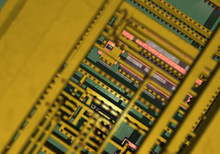
Synthetic detail of a micromanufactured integrated circuit through four layers of planarized copper interconnect, down to the polysilicon (pink), wells (greyish) and substrate (green)
Microfabrication is the process of fabricating miniature structures of micrometre scales and smaller. Historically, the earliest microfabrication processes were used for integrated circuit fabrication, also known as "semiconductor manufacturing" or "semiconductor device fabrication". In the last two decades, microelectromechanical systems (MEMS), microsystems (European usage), micromachines (Japanese terminology) and their subfields have re-used, adapted or extended microfabrication methods. These subfields include microfluidics/lab-on-a-chip, optical MEMS (also called MOEMS), RF MEMS, PowerMEMS, BioMEMS and their extension into nanoscale (for example NEMS, for nano electro mechanical systems). The production of flat-panel displays and solar cells also uses similar techniques.
Miniaturization of various devices presents challenges in many areas of science and engineering: physics, chemistry, materials science, computer science, ultra-precision engineering, fabrication processes, and equipment design. It is also giving rise to various kinds of interdisciplinary research.[1] The major concepts and principles of microfabrication are microlithography, doping, thin films, etching, bonding, and polishing.
Simplified illustration of the process of fabrication of a CMOS inverter on p-type substrate in semiconductor microfabrication. Each etch step is detailed in the following image. The diagrams are not to scale, as in real devices, the gate, source, and drain contacts are not normally located in the same plane.Detail of an etch step.
Microfabrication technologies originate from the microelectronics industry, and the devices are usually made on silicon wafers even though glass, plastics and many other substrate are in use. Micromachining, semiconductor processing, microelectronic fabrication, semiconductor fabrication, MEMS fabrication and integrated circuit technology are terms used instead of microfabrication, but microfabrication is the broad general term.
Traditional machining techniques such as electro-discharge machining, spark erosion machining, and laser drilling have been scaled from the millimeter size range to micrometer range, but they do not share the main idea of microelectronics-originated microfabrication: replication and parallel fabrication of hundreds or millions of identical structures. This parallelism is present in various imprint, casting and moulding techniques which have successfully been applied in the microregime. For example, injection moulding of DVDs involves fabrication of submicrometer-sized spots on the disc.
To fabricate a microdevice, many processes must be performed, one after the other, many times repeatedly. These processes typically include depositing a film, patterning the film with the desired micro features, and removing (or etching) portions of the film. Thin film metrology is used typically during each of these individual process steps, to ensure the film structure has the desired characteristics in terms of thickness (t), refractive index (n) and extinction coefficient (k),[2] for suitable device behavior. For example, in memory chip fabrication there are some 30 lithography steps, 10 oxidation steps, 20 etching steps, 10 doping steps, and many others are performed. The complexity of microfabrication processes can be described by their mask count. This is the number of different pattern layers that constitute the final device. Modern microprocessors are made with 30 masks while a few masks suffice for a microfluidic device or a laser diode. Microfabrication resembles multiple exposure photography, with many patterns aligned to each other to create the final structure.
Substrates
Microfabricated devices are not generally freestanding devices but are usually formed over or in a thicker support substrate. For electronic applications, semiconducting substrates such as silicon wafers can be used. For optical devices or flat panel displays, transparent substrates such as glass or quartz are common. The substrate enables easy handling of the micro device through the many fabrication steps. Often many individual devices are made together on one substrate and then singulated into separated devices toward the end of fabrication.
Deposition or growth
Microfabricated devices are typically constructed using one or more thin films (see Thin film deposition). The purpose of these thin films depends upon the type of device. Electronic devices may have thin films which are conductors (metals), insulators (dielectrics) or semiconductors. Optical devices may have films which are reflective, transparent, light guiding or scattering. Films may also have a chemical or mechanical purpose as well as for MEMS applications. Examples of deposition techniques include:
It is often desirable to pattern a film into distinct features or to form openings (or vias) in some of the layers. These features are on the micrometer or nanometer scale and the patterning technology is what defines microfabrication. This patterning technique typically uses a 'mask' to define portions of the film which will be removed. Examples of patterning techniques include:
Etching is the removal of some portion of the thin film or substrate. The substrate is exposed to an etching (such as an acid or plasma) which chemically or physically attacks the film until it is removed. Etching techniques include:
Microforming is a microfabrication process of microsystem or microelectromechanical system (MEMS) "parts or structures with at least two dimensions in the submillimeter range."[3][4][5] It includes techniques such as microextrusion,[4]microstamping,[6] and microcutting.[7] These and other microforming processes have been envisioned and researched since at least 1990,[3] leading to the development of industrial- and experimental-grade manufacturing tools. However, as Fu and Chan pointed out in a 2013 state-of-the-art technology review, several issues must still be resolved before the technology can be implemented more widely, including deformation load and defects, forming system stability, mechanical properties, and other size-related effects on the crystallite (grain) structure and boundaries:[4][5][8]
In microforming, the ratio of the total surface area of grain boundaries to the material volume decreases with the decrease of specimen size and the increase of grain size. This leads to the decrease of grain boundary strengthening effect. Surface grains have lesser constraints compared to internal grains. The change of flow stress with part geometry size is partly attributed to the change of volume fraction of surface grains. In addition, the anisotropic properties of each grain become significant with the decrease of workpiece size, which results in the inhomogeneous deformation, irregular formed geometry and the variation of deformation load. There is a critical need to establish the systematic knowledge of microforming to support the design of part, process, and tooling with the consideration of size effects.[8]
Other
a wide variety of other processes for cleaning, planarizing, or modifying the chemical properties of microfabricated devices can also be performed. Some examples include:
Microfabrication is carried out in cleanrooms, where air has been filtered of particle contamination and temperature, humidity, vibrations and electrical disturbances are under stringent control. Smoke, dust, bacteria and cells are micrometers in size, and their presence will destroy the functionality of a microfabricated device.
Cleanrooms provide passive cleanliness but the wafers are also actively cleaned before every critical step. RCA-1 clean in ammonia-peroxide solution removes organic contamination and particles; RCA-2 cleaning in hydrogen chloride-peroxide mixture removes metallic impurities. Sulfuric acid-peroxide mixture (a.k.a. Piranha) removes organics. Hydrogen fluoride removes native oxide from silicon surface. These are all wet cleaning steps in solutions. Dry cleaning methods include oxygen and argon plasma treatments to remove unwanted surface layers, or hydrogen bake at elevated temperature to remove native oxide before epitaxy. Pre-gate cleaning is the most critical cleaning step in CMOS fabrication: it ensures that the ca. 2nm thick oxide of a MOS transistor can be grown in an orderly fashion. Oxidation, and all high temperature steps are very sensitive to contamination, and cleaning steps must precede high temperature steps.
Surface preparation is just a different viewpoint, all the steps are the same as described above: it is about leaving the wafer surface in a controlled and well known state before you start processing. Wafers are contaminated by previous process steps (e.g. metals bombarded from chamber walls by energetic ions during ion implantation), or they may have gathered polymers from wafer boxes, and this might be different depending on wait time.
Wafer cleaning and surface preparation work similarly to the machines in a bowling alley: first they remove all unwanted bits and pieces, and then they reconstruct the desired pattern so that the game can go on.
1 2 Engel, U.; Eckstein, R. (2002). "Microforming - From Basic research to its realization". Journal of Materials Processing Technology. 125–126 (2002): 35–44. doi:10.1016/S0924-0136(02)00415-6.
↑ Fu, M.W.; Chan, W.L. (2014). "Chapter 4: Microforming Processes". Micro-scaled Products Development via Microforming: Deformation Behaviours, Processes, Tooling and its Realization. Springer Science & Business Media. pp.73–130. ISBN9781447163268.
1 2 Fu, M.W.; Chan, W.L. (2013). "A review on the state-of-the-art microforming technologies". International Journal of Advanced Manufacturing Technology. 67 (9): 2411–2437. doi:10.1007/s00170-012-4661-7. S2CID110879846.
This page is based on this Wikipedia article Text is available under the CC BY-SA 4.0 license; additional terms may apply. Images, videos and audio are available under their respective licenses.