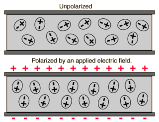
In electromagnetism, a dielectric is an electrical insulator that can be polarised by an applied electric field. When a dielectric material is placed in an electric field, electric charges do not flow through the material as they do in an electrical conductor, because they have no loosely bound, or free, electrons that may drift through the material, but instead they shift, only slightly, from their average equilibrium positions, causing dielectric polarisation. Because of dielectric polarisation, positive charges are displaced in the direction of the field and negative charges shift in the direction opposite to the field. This creates an internal electric field that reduces the overall field within the dielectric itself. If a dielectric is composed of weakly bonded molecules, those molecules not only become polarised, but also reorient so that their symmetry axes align to the field.
In electrical engineering, electrical length is a dimensionless parameter equal to the physical length of an electrical conductor such as a cable or wire, divided by the wavelength of alternating current at a given frequency traveling through the conductor. In other words, it is the length of the conductor measured in wavelengths. It can alternately be expressed as an angle, in radians or degrees, equal to the phase shift the alternating current experiences traveling through the conductor.
In electromagnetism, the absolute permittivity, often simply called permittivity and denoted by the Greek letter ε (epsilon), is a measure of the electric polarizability of a dielectric. A material with high permittivity polarizes more in response to an applied electric field than a material with low permittivity, thereby storing more energy in the material. In electrostatics, the permittivity plays an important role in determining the capacitance of a capacitor.

Capacitance is the capability of a material object or device to store electric charge. It is measured by the charge in response to a difference in electric potential, expressed as the ratio of those quantities. Commonly recognized are two closely related notions of capacitance: self capacitance and mutual capacitance. An object that can be electrically charged exhibits self capacitance, for which the electric potential is measured between the object and ground. Mutual capacitance is measured between two components, and is particularly important in the operation of the capacitor, an elementary linear electronic component designed to add capacitance to an electric circuit.
Ferroelectric capacitor is a capacitor based on a ferroelectric material. In contrast, traditional capacitors are based on dielectric materials. Ferroelectric devices are used in digital electronics as part of ferroelectric RAM, or in analog electronics as tunable capacitors (varactors).

In physics, the electric displacement field or electric induction is a vector field that appears in Maxwell's equations. It accounts for the electromagnetic effects of polarization and that of an electric field, combining the two in an auxiliary field. It plays a major role in topics such as the capacitance of a material, as well the response of dielectrics to electric field, and how shapes can change due to electric fields in piezoelectricity or flexoelectricity as well as the creation of voltages and charge transfer due to elastic strains.
In semiconductor physics, the depletion region, also called depletion layer, depletion zone, junction region, space charge region, or space charge layer, is an insulating region within a conductive, doped semiconductor material where the mobile charge carriers have diffused away, or forced away by an electric field. The only elements left in the depletion region are ionized donor or acceptor impurities. This region of uncovered positive and negative ions is called the depletion region due to the depletion of carriers in this region, leaving none to carry a current. Understanding the depletion region is key to explaining modern semiconductor electronics: diodes, bipolar junction transistors, field-effect transistors, and variable capacitance diodes all rely on depletion region phenomena.
Electric potential energy is a potential energy that results from conservative Coulomb forces and is associated with the configuration of a particular set of point charges within a defined system. An object may be said to have electric potential energy by virtue of either its own electric charge or its relative position to other electrically charged objects.

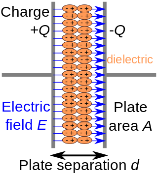
Capacitors are manufactured in many styles, forms, dimensions, and from a large variety of materials. They all contain at least two electrical conductors, called plates, separated by an insulating layer (dielectric). Capacitors are widely used as parts of electrical circuits in many common electrical devices.

In electrical engineering, a capacitor is a device that stores electrical energy by accumulating electric charges on two closely spaced surfaces that are insulated from each other. It is a passive electronic component with two terminals.
In electrical engineering, dielectric loss quantifies a dielectric material's inherent dissipation of electromagnetic energy. It can be parameterized in terms of either the loss angleδ or the corresponding loss tangenttan(δ). Both refer to the phasor in the complex plane whose real and imaginary parts are the resistive (lossy) component of an electromagnetic field and its reactive (lossless) counterpart.

Dielectric elastomers (DEs) are smart material systems that produce large strains and are promising for Soft robotics, Artificial muscle, etc. They belong to the group of electroactive polymers (EAP). DE actuators (DEA) transform electric energy into mechanical work and vice versa. Thus, they can be used as both actuators, sensors, and energy-harvesting devices. They have high elastic energy density and fast response due to being lightweight, highly stretchable, and operating under the electrostatic principle. They have been investigated since the late 1990s. Many prototype applications exist. Every year, conferences are held in the US and Europe.

A ceramic capacitor is a fixed-value capacitor where the ceramic material acts as the dielectric. It is constructed of two or more alternating layers of ceramic and a metal layer acting as the electrodes. The composition of the ceramic material defines the electrical behavior and therefore applications. Ceramic capacitors are divided into two application classes:

A radio-frequency microelectromechanical system is a microelectromechanical system with electronic components comprising moving sub-millimeter-sized parts that provide radio-frequency (RF) functionality. RF functionality can be implemented using a variety of RF technologies. Besides RF MEMS technology, III-V compound semiconductor, ferrite, ferroelectric, silicon-based semiconductor, and vacuum tube technology are available to the RF designer. Each of the RF technologies offers a distinct trade-off between cost, frequency, gain, large-scale integration, lifetime, linearity, noise figure, packaging, power handling, power consumption, reliability, ruggedness, size, supply voltage, switching time and weight.

A supercapacitor (SC), also called an ultracapacitor, is a high-capacity capacitor, with a capacitance value much higher than solid-state capacitors but with lower voltage limits. It bridges the gap between electrolytic capacitors and rechargeable batteries. It typically stores 10 to 100 times more energy per unit volume or mass than electrolytic capacitors, can accept and deliver charge much faster than batteries, and tolerates many more charge and discharge cycles than rechargeable batteries.
The history of electrovibration goes back to 1954. It was first discovered by accident and E. Mallinckrodt, A. L. Hughes and W. Sleator Jr. reported “... that dragging a dry finger over a conductive surface covered with a thin insulating layer and excited with a 110 V signal, created a characteristic rubbery feeling”. In their experiment, the finger and the metal surface create a capacitive setup. The attraction force created between the finger and the surface was too weak to perceive, but it generated a rubbery sensation when the finger was moving on the surface. This sensation was named "electrovibration" by the group. From around early 2010 Senseg and Disney Research are developing technology that could bring electrovibration to modern touchscreen devices.
Double-layer capacitance is the important characteristic of the electrical double layer which appears at the interface between a surface and a fluid. At this boundary two layers of electric charge with opposing polarity form, one at the surface of the electrode, and one in the electrolyte. These two layers, electrons on the electrode and ions in the electrolyte, are typically separated by a single layer of solvent molecules that adhere to the surface of the electrode and act like a dielectric in a conventional capacitor. The amount of charge stored in double-layer capacitor depends on the applied voltage.
Three-dimensional electrical capacitance tomography also known as electrical capacitance volume tomography (ECVT) is a non-invasive 3D imaging technology applied primarily to multiphase flows. Was introduced in the early 2000s as an extension of the conventional two-dimensional ECT. In conventional electrical capacitance tomography, sensor plates are distributed around a surface of interest. Measured capacitance between plate combinations is used to reconstruct 2D images (tomograms) of material distribution. Because the ECT sensor plates are required to have lengths on the order of the domain cross-section, 2D ECT does not provide the required resolution in the axial dimension. In ECT, the fringing field from the edges of the plates is viewed as a source of distortion to the final reconstructed image and is thus mitigated by guard electrodes. 3D ECT exploits this fringing field and expands it through 3D sensor designs that deliberately establish an electric field variation in all three dimensions. In 3D tomography, the data are acquired in 3D geometry, and the reconstruction algorithm produces the three-dimensional image directly, in contrast to 2D tomography, where 3D information might be obtained by stacking 2D slices reconstructed individually.

In semiconductor electrochemistry, a Mott–Schottky plot describes the reciprocal of the square of capacitance versus the potential difference between bulk semiconductor and bulk electrolyte. In many theories, and in many experimental measurements, the plot is linear. The use of Mott–Schottky plots to determine system properties is termed Mott–Schottky analysis.
Performance modelling is the abstraction of a real system into a simplified representation to enable the prediction of performance. The creation of a model can provide insight into how a proposed or actual system will or does work. This can, however, point towards different things to people belonging to different fields of work.


