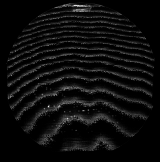
Microelectromechanical systems (MEMS), also written as micro-electro-mechanical systems and the related micromechatronics and microsystems constitute the technology of microscopic devices, particularly those with moving parts. They merge at the nanoscale into nanoelectromechanical systems (NEMS) and nanotechnology. MEMS are also referred to as micromachines in Japan and microsystem technology (MST) in Europe.
Bulk micromachining is a process used to produce micromachinery or microelectromechanical systems (MEMS).
In semiconductor fabrication, a resist is a thin layer used to transfer a circuit pattern to the semiconductor substrate which it is deposited upon. A resist can be patterned via lithography to form a (sub)micrometer-scale, temporary mask that protects selected areas of the underlying substrate during subsequent processing steps. The material used to prepare said thin layer is typically a viscous solution. Resists are generally proprietary mixtures of a polymer or its precursor and other small molecules that have been specially formulated for a given lithography technology. Resists used during photolithography are called photoresists.
Deep reactive-ion etching (DRIE) is a highly anisotropic etch process used to create deep penetration, steep-sided holes and trenches in wafers/substrates, typically with high aspect ratios. It was developed for microelectromechanical systems (MEMS), which require these features, but is also used to excavate trenches for high-density capacitors for DRAM and more recently for creating through silicon vias (TSVs) in advanced 3D wafer level packaging technology.

Microfabrication is the process of fabricating miniature structures of micrometre scales and smaller. Historically, the earliest microfabrication processes were used for integrated circuit fabrication, also known as "semiconductor manufacturing" or "semiconductor device fabrication". In the last two decades microelectromechanical systems (MEMS), microsystems, micromachines and their subfields, microfluidics/lab-on-a-chip, optical MEMS, RF MEMS, PowerMEMS, BioMEMS and their extension into nanoscale have re-used, adapted or extended microfabrication methods. Flat-panel displays and solar cells are also using similar techniques.

Etching is used in microfabrication to chemically remove layers from the surface of a wafer during manufacturing. Etching is a critically important process module, and every wafer undergoes many etching steps before it is complete.
A plasma etcher, or etching tool, is a tool used in the production of semiconductor devices. A plasma etcher produces a plasma from a process gas, typically oxygen or a fluorine-bearing gas, using a high frequency electric field, typically 13.56 MHz. A silicon wafer is placed in the plasma etcher, and the air is evacuated from the process chamber using a system of vacuum pumps. Then a process gas is introduced at low pressure, and is excited into a plasma through dielectric breakdown.
Microoptoelectromechanical systems (MOEMS), also written as micro-opto-electro-mechanical systems or micro-optoelectromechanical systems, also known as optical microelectromechanical systems or optical MEMS, are not a special class of microelectromechanical systems (MEMS) but rather the combination of MEMS merged with micro-optics; this involves sensing or manipulating optical signals on a very small size scale using integrated mechanical, optical, and electrical systems. MOEMS includes a wide variety of devices, for example optical switch, optical cross-connect, tunable VCSEL, microbolometers. These devices are usually fabricated using micro-optics and standard micromachining technologies using materials like silicon, silicon dioxide, silicon nitride and gallium arsenide.
Adhesive bonding describes a wafer bonding technique with applying an intermediate layer to connect substrates of different types of materials. Those connections produced can be soluble or insoluble. The commercially available adhesive can be organic or inorganic and is deposited on one or both substrate surfaces. Adhesives, especially the well-established SU-8, and benzocyclobutene (BCB), are specialized for MEMS or electronic component production.
The lift-off process in microstructuring technology is a method of creating structures (patterning) of a target material on the surface of a substrate using a sacrificial material . It is an additive technique as opposed to more traditional subtracting technique like etching. The scale of the structures can vary from the nanoscale up to the centimeter scale or further, but are typically of micrometric dimensions.

Beam lead technology is a method of fabricating a semiconductor device. Its original application was to high-frequency silicon switching transistors and high-speed integrated circuits. It eliminated the labor-intensive wire-bonding process used for integrated circuits at the time and allowed automated assembly of semiconductor chips onto larger substrates to produce hybrid integrated circuits.
Thermocompression bonding describes a wafer bonding technique and is also referred to as diffusion bonding, pressure joining, thermocompression welding or solid-state welding. Two metals, e.g. gold (Au)-gold (Au), are brought into atomic contact applying force and heat simultaneously. The diffusion requires atomic contact between the surfaces due to the atomic motion. The atoms migrate from one crystal lattice to the other one based on crystal lattice vibration. This atomic interaction sticks the interface together. The diffusion process is described by the following three processes:
A capacitive micromachined ultrasonic transducer (CMUT) is a relatively new concept in the field of ultrasonic transducers. Most of the commercial ultrasonic transducers today are based on piezoelectricity. CMUTs are the transducers where the energy transduction is due to change in capacitance. CMUTs are constructed on silicon using micromachining techniques. A cavity is formed in a silicon substrate, and a thin layer suspended on the top of the cavity serves as a membrane on which a metallized layer acts an electrode, together with the silicon substrate which serves as a bottom electrode.
Anodic bonding is a wafer bonding process to seal glass to either silicon or metal without introducing an intermediate layer; it is commonly used to seal glass to silicon wafers in electronics and microfluidics. This bonding technique, also known as field assisted bonding or electrostatic sealing, is mostly used for connecting silicon/glass and metal/glass through electric fields. The requirements for anodic bonding are clean and even wafer surfaces and atomic contact between the bonding substrates through a sufficiently powerful electrostatic field. Also necessary is the use of borosilicate glass containing a high concentration of alkali ions. The coefficient of thermal expansion (CTE) of the processed glass needs to be similar to those of the bonding partner.

Eutectic bonding, also referred to as eutectic soldering, describes a wafer bonding technique with an intermediate metal layer that can produce a eutectic system. Those eutectic metals are alloys that transform directly from solid to liquid state, or vice versa from liquid to solid state, at a specific composition and temperature without passing a two-phase equilibrium, i.e. liquid and solid state. The fact that the eutectic temperature can be much lower than the melting temperature of the two or more pure elements can be important in eutectic bonding.
Microelectromechanical system oscillators are timing devices that generate highly stable reference frequencies, which can measure time. These reference frequencies may be used to sequence electronic systems, manage data transfer, define radio frequencies, and measure elapsed time. The core technologies used in MEMS oscillators have been in development since the mid-1960s, but have only been sufficiently advanced for commercial applications since 2006. MEMS oscillators incorporate MEMS resonators, which are microelectromechanical structures that define stable frequencies. MEMS clock generators are MEMS timing devices with multiple outputs for systems that need more than a single reference frequency. MEMS oscillators are a valid alternative to older, more established quartz crystal oscillators, offering better resilience against vibration and mechanical shock, and reliability with respect to temperature variation.

Richard Stephen Muller is an American professor in the Electrical Engineering and Computer Science Department of the University of California at Berkeley. He made contributions to the founding and growth of the field of MicroElectromechanical Systems (MEMS). Together with student, Roger T. Howe, he made the initial seminal contribution of polysilicon sacrificially-released beams in 1982. This led to a class of micromanufacturing processes called surface micromachining. These processes preceded the creation of low cost, mass-produced commercial micro accelerometers, which are used in automotive collision sensors for airbag deployment. Together with Richard M. White, he created BSAC, an organization that produced many generations of academic researchers and intellectual properties in the MEMS field. MEMS is an activity that in 2013 accounted for multi-billion dollar revenue worldwide. He is a member of the US National Academy of Engineering.
A nanoelectromechanical (NEM) relay is an electrically actuatedswitch that is built on the nanometer scale using semiconductor fabrication techniques. They are designed to operate in replacement, or in conjunction, with traditional semiconductor logic. While the mechanical nature of NEM relays makes them switch much slower than solid-state relays, they have many advantageous properties, such as zero current leakage and low power consumption, which make them potentially useful in next generation computing.
A piezoelectric microelectromechanical system (piezoMEMS) is a miniature or microscopic device that uses piezoelectricity to generate motion and carry out its tasks. It is a microelectromechanical system that takes advantage of an electrical potential that appears under mechanical stress. PiezoMEMS can be found in a variety of applications, such as switches, inkjet printer heads, sensors, micropumps, and energy harvesters.
Vapor etching refers to a process used in the fabrication of Microelectromechanical systems (MEMS) and Nanoelectromechanical systems (NEMS). Sacrificial layers are isotropically etched using gaseous acids such as Hydrogen fluoride and Xenon difluoride to release the free standing components of the device.


