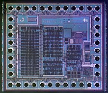
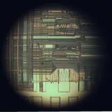
A microscope image of an integrated circuit die used to control LCDs. The pinouts are the dark circles surrounding the integrated circuit.
An integrated circuit (IC), also known as a microchip or simply chip, is a set of electronic circuits, consisting of various electronic components (such as transistors, resistors, and capacitors) and their interconnections.[1] These components are etched onto a small, flat piece ("chip") of semiconductor material, usually silicon.[1] Integrated circuits are used in a wide range of electronic devices, including computers, smartphones, and televisions, to perform various functions such as processing and storing information. They have greatly impacted the field of electronics by enabling device miniaturization and enhanced functionality.
Integrated circuits are orders of magnitude smaller, faster, and less expensive than those constructed of discrete components, allowing a large transistor count.
The IC's mass production capability, reliability, and building-block approach to integrated circuit design have ensured the rapid adoption of standardized ICs in place of designs using discrete transistors. ICs are now used in virtually all electronic equipment and have revolutionized the world of electronics. Computers, mobile phones, and other home appliances are now essential parts of the structure of modern societies, made possible by the small size and low cost of ICs such as modern computer processors and microcontrollers.
Very-large-scale integration was made practical by technological advancements in semiconductor device fabrication. Since their origins in the 1960s, the size, speed, and capacity of chips have progressed enormously, driven by technical advances that fit more and more transistors on chips of the same size– a modern chip may have many billions of transistors in an area the size of a human fingernail. These advances, roughly following Moore's law, make the computer chips of today possess millions of times the capacity and thousands of times the speed of the computer chips of the early 1970s.
ICs have three main advantages over circuits constructed out of discrete components:size, cost and performance. The size and cost is low because the chips, with all their components, are printed as a unit by photolithography rather than being constructed one transistor at a time. Furthermore, packaged ICs use much less material than discrete circuits. Performance is high because the IC's components switch quickly and consume comparatively little power because of their small size and proximity. The main disadvantage of ICs is the high initial cost of designing them and the enormous capital cost of factory construction. This high initial cost means ICs are only commercially viable when high production volumes are anticipated.
A circuit in which all or some of the circuit elements are inseparably associated and electrically interconnected so that it is considered to be indivisible for the purposes of construction and commerce.
In strict usage, integrated circuit refers to the single-piece circuit construction originally known as a monolithic integrated circuit, which comprises a single piece of silicon.[3][4] In general usage, circuits not meeting this strict definition are sometimes referred to as ICs, which are constructed using many different technologies, e.g. 3D IC, 2.5D IC, MCM, thin-film transistors, thick-film technologies, or hybrid integrated circuits. The choice of terminology frequently appears in discussions related to whether Moore's Law is obsolete.
Jack Kilby's original integrated circuit; the world's first. Made from germanium with gold-wire interconnects.
History
An early attempt at combining several components in one device (like modern ICs) was the Loewe 3NF vacuum tube first made in 1926.[5][6] Unlike ICs, it was designed with the purpose of tax avoidance, as in Germany, radio receivers had a tax that was levied depending on how many tube holders a radio receiver had. It allowed radio receivers to have a single tube holder. One million were manufactured, and were "a first step in integration of radioelectronic devices".[7] The device contained an amplifier, composed of three triodes, two capacitors and four resistors in a six-pin device.[8] Radios with the Loewe 3NF were less expensive than other radios,[9] showing one of the advantages of integration over using discrete components, that would be seen decades later with ICs.[10]
Early concepts of an integrated circuit go back to 1949, when German engineer Werner Jacobi[11] (SiemensAG)[12] filed a patent for an integrated-circuit-like semiconductor amplifying device[13] showing five transistors on a common substrate in a three-stage amplifier arrangement. Jacobi disclosed small and cheap hearing aids as typical industrial applications of his patent. An immediate commercial use of his patent has not been reported.
Another early proponent of the concept was Geoffrey Dummer (1909–2002), a radar scientist working for the Royal Radar Establishment of the British Ministry of Defence. Dummer presented the idea to the public at the Symposium on Progress in Quality Electronic Components in Washington,D.C., on 7 May 1952.[14] He gave many symposia publicly to propagate his ideas and unsuccessfully attempted to build such a circuit in 1956. Between 1953 and 1957, Sidney Darlington and Yasuo Tarui (Electrotechnical Laboratory) proposed similar chip designs where several transistors could share a common active area, but there was no electrical isolation to separate them from each other.[11]
The monolithic integrated circuit chip was enabled by the inventions of the planar process by Jean Hoerni and p–n junction isolation by Kurt Lehovec. Hoerni's invention was built on Carl Frosch and Lincoln Derick's work on surface protection and passivation by silicon dioxide masking and predeposition,[15][16][17] as well as Fuller, Ditzenberger's and others work on the diffusion of impurities into silicon. [18][19][20][21][22]
Robert Noyce invented the first monolithic integrated circuit in 1959. The chip was made from silicon.
A precursor idea to the IC was to create small ceramic substrates (so-called micromodules),[23] each containing a single miniaturized component. Components could then be integrated and wired into a bidimensional or tridimensional compact grid. This idea, which seemed very promising in 1957, was proposed to the US Army by Jack Kilby[23] and led to the short-lived Micromodule Program (similar to 1951's Project Tinkertoy).[23][24][25] However, as the project was gaining momentum, Kilby came up with a new, revolutionary design: theIC.
Newly employed by Texas Instruments, Kilby recorded his initial ideas concerning the integrated circuit in July 1958, successfully demonstrating the first working example of an integrated circuit on 12 September 1958.[26] In his patent application of 6 February 1959,[27] Kilby described his new device as "a body of semiconductor material … wherein all the components of the electronic circuit are completely integrated".[28] The first customer for the new invention was the US Air Force.[29] Kilby won the 2000 Nobel Prize in physics for his part in the invention of the integrated circuit.[30]
However, Kilby's invention was not a true monolithic integrated circuit chip since it had external gold-wire connections, which would have made it difficult to mass-produce.[31] Half a year after Kilby, Robert Noyce at Fairchild Semiconductor invented the first true monolithic IC chip.[32][31] More practical than Kilby's implementation, Noyce's chip was made of silicon, whereas Kilby's was made of germanium, and Noyce's was fabricated using the planar process, developed in early 1959 by his colleague Jean Hoerni and included the critical on-chip aluminum interconnecting lines. Modern IC chips are based on Noyce's monolithic IC,[32][31] rather than Kilby's.
NASA's Apollo Program was the largest single consumer of integrated circuits between 1961 and 1965.[33]
Nearly all modern IC chips are metal–oxide–semiconductor (MOS) integrated circuits, built from MOSFETs (metal–oxide–silicon field-effect transistors).[36] The MOSFET invented at Bell Labs between 1955 and 1960,[37][38][39][40][41][42][43] made it possible to build high-density integrated circuits.[44] In contrast to bipolar transistors which required a number of steps for the p–n junction isolation of transistors on a chip, MOSFETs required no such steps but could be easily isolated from each other.[45] Its advantage for integrated circuits was pointed out by Dawon Kahng in 1961.[46] The list of IEEE milestones includes the first integrated circuit by Kilby in 1958,[47] Hoerni's planar process and Noyce's planar IC in 1959.[48]
The earliest experimental MOS IC to be fabricated was a 16-transistor chip built by Fred Heiman and Steven Hofstein at RCA in 1962.[49]General Microelectronics later introduced the first commercial MOS integrated circuit in 1964,[50] a 120-transistor shift register developed by Robert Norman.[49] By 1964, MOS chips had reached higher transistor density and lower manufacturing costs than bipolar chips. MOS chips further increased in complexity at a rate predicted by Moore's law, leading to large-scale integration (LSI) with hundreds of transistors on a single MOS chip by the late 1960s.[51]
Following the development of the self-aligned gate (silicon-gate) MOSFET by Robert Kerwin, Donald Klein and John Sarace at Bell Labs in 1967,[52] the first silicon-gate MOS IC technology with self-aligned gates, the basis of all modern CMOS integrated circuits, was developed at Fairchild Semiconductor by Federico Faggin in 1968.[53] The application of MOS LSI chips to computing was the basis for the first microprocessors, as engineers began recognizing that a complete computer processor could be contained on a single MOS LSI chip. This led to the inventions of the microprocessor and the microcontroller by the early 1970s.[51] During the early 1970s, MOS integrated circuit technology enabled the very large-scale integration (VLSI) of more than 10,000 transistors on a single chip.[54]
At first, MOS-based computers only made sense when high density was required, such as aerospace and pocket calculators. Computers built entirely from TTL, such as the 1970 Datapoint 2200, were much faster and more powerful than single-chip MOS microprocessors such as the 1972 Intel 8008 until the early 1980s.[35]
Advances in IC technology, primarily smaller features and larger chips, have allowed the number of MOS transistors in an integrated circuit to double every two years, a trend known as Moore's law. Moore originally stated it would double every year, but he went on to change the claim to every two years in 1975.[55] This increased capacity has been used to decrease cost and increase functionality. In general, as the feature size shrinks, almost every aspect of an IC's operation improves. The cost per transistor and the switching power consumption per transistor goes down, while the memory capacity and speed go up, through the relationships defined by Dennard scaling (MOSFET scaling).[56] Because speed, capacity, and power consumption gains are apparent to the end user, there is fierce competition among the manufacturers to use finer geometries. Over the years, transistor sizes have decreased from tens of microns in the early 1970s to 10 nanometers in 2017[57] with a corresponding million-fold increase in transistors per unit area. As of 2016, typical chip areas range from a few square millimeters to around 600mm2, with up to 25 million transistors per mm2.[58]
Initially, ICs were strictly electronic devices. The success of ICs has led to the integration of other technologies, in an attempt to obtain the same advantages of small size and low cost. These technologies include mechanical devices, optics, and sensors.
Charge-coupled devices, and the closely related active-pixel sensors, are chips that are sensitive to light. They have largely replaced photographic film in scientific, medical, and consumer applications. Billions of these devices are now produced each year for applications such as cellphones, tablets, and digital cameras. This sub-field of ICs won the Nobel Prize in 2009.[60]
Since the early 2000s, the integration of optical functionality (optical computing) into silicon chips has been actively pursued in both academic research and in industry resulting in the successful commercialization of silicon based integrated optical transceivers combining optical devices (modulators, detectors, routing) with CMOS based electronics.[62]Photonic integrated circuits that use light such as Lightelligence's PACE (Photonic Arithmetic Computing Engine) also being developed, using the emerging field of physics known as photonics.[63]
Integrated circuits are also being developed for sensor applications in medical implants or other bioelectronic devices.[64] Special sealing techniques have to be applied in such biogenic environments to avoid corrosion or biodegradation of the exposed semiconductor materials.[65]
As of 2018[update], the vast majority of all transistors are MOSFETs fabricated in a single layer on one side of a chip of silicon in a flat two-dimensional planar process. Researchers have produced prototypes of several promising alternatives, such as:
As it becomes more difficult to manufacture ever smaller transistors, companies are using multi-chip modules/chiplets, three-dimensional integrated circuits, package on package, High Bandwidth Memory and through-silicon vias with die stacking to increase performance and reduce size, without having to reduce the size of the transistors. Such techniques are collectively known as advanced packaging.[70] Advanced packaging is mainly divided into 2.5D and 3D packaging. 2.5D describes approaches such as multi-chip modules while 3D describes approaches where dies are stacked in one way or another, such as package on package and high bandwidth memory. All approaches involve 2 or more dies in a single package.[71][72][73][74][75] Alternatively, approaches such as 3D NAND stack multiple layers on a single die. A technique has been demonstrated to include microfluidic cooling on integrated circuits, to improve cooling performance[76] as well as peltier thermoelectric coolers on solder bumps, or thermal solder bumps used exclusively for heat dissipation, used in flip-chip.[77][78]
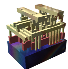
Virtual detail of an integrated circuit through four layers of planarized copper interconnect, down to the polysilicon (pink), wells (greyish), and substrate (green)
The cost of designing and developing a complex integrated circuit is quite high, normally in the multiple tens of millions of dollars.[79][80] Therefore, it only makes economic sense to produce integrated circuit products with high production volume, so the non-recurring engineering (NRE) costs are spread across typically millions of production units.
Modern semiconductor chips have billions of components, and are far too complex to be designed by hand. Software tools to help the designer are essential. Electronic design automation (EDA), also referred to as electronic computer-aided design (ECAD),[81] is a category of software tools for designing electronic systems, including integrated circuits. The tools work together in a design flow that engineers use to design, verify, and analyze entire semiconductor chips. Some of the latest EDA tools use artificial intelligence (AI) to help engineers save time and improve chip performance.
Integrated circuits can be broadly classified into analog,[82]digital[83] and mixed signal,[84] consisting of analog and digital signaling on the same IC.
Among the most advanced integrated circuits are the microprocessors or "cores", used in personal computers, cell-phones, etc. Several cores may be integrated together in a single IC or chip. Digital memory chips and application-specific integrated circuits (ASICs) are examples of other families of integrated circuits.
In the 1980s, programmable logic devices were developed. These devices contain circuits whose logical function and connectivity can be programmed by the user, rather than being fixed by the integrated circuit manufacturer. This allows a chip to be programmed to do various LSI-type functions such as logic gates, adders and registers. Programmability comes in various forms – devices that can be programmed only once, devices that can be erased and then re-programmed using UV light, devices that can be (re)programmed using flash memory, and field-programmable gate arrays (FPGAs) which can be programmed at any time, including during operation. Current FPGAs can (as of 2016) implement the equivalent of millions of gates and operate at frequencies up to 1 GHz.[85]
ICs can combine analog and digital circuits on a chip to create functions such as analog-to-digital converters and digital-to-analog converters. Such mixed-signal circuits offer smaller size and lower cost, but must account for signal interference. Prior to the late 1990s, radios could not be fabricated in the same low-cost CMOS processes as microprocessors. But since 1998, radio chips have been developed using RF CMOS processes. Examples include Intel's DECT cordless phone, or 802.11 (Wi-Fi) chips created by Atheros and other companies.[86]
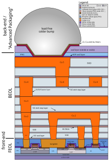
Rendering of a small standard cell with three metal layers (dielectric has been removed). The sand-colored structures are metal interconnect, with the vertical pillars being contacts, typically plugs of tungsten. The reddish structures are polysilicon gates, and the solid at the bottom is the crystalline silicon bulk.Schematic structure of a CMOS chip, as built in the early 2000s. The graphic shows LDD-MISFET's on an SOI substrate with five metallization layers and solder bump for flip-chip bonding. It also shows the section for FEOL (front-end of line), BEOL (back-end of line) and first parts of back-end process.
Semiconductor ICs are fabricated in a planar process which includes three key process steps–photolithography, deposition (such as chemical vapor deposition), and etching. The main process steps are supplemented by doping and cleaning. More recent or high-performance ICs may instead use multi-gateFinFET or GAAFET transistors instead of planar ones, starting at the 22nm node (Intel) or 16/14nm nodes.[87]
Mono-crystal siliconwafers are used in most applications (or for special applications, other semiconductors such as gallium arsenide are used). The wafer need not be entirely silicon. Photolithography is used to mark different areas of the substrate to be doped or to have polysilicon, insulators or metal (typically aluminium or copper) tracks deposited on them. Dopants are impurities intentionally introduced to a semiconductor to modulate its electronic properties. Doping is the process of adding dopants to a semiconductor material.
Integrated circuits are composed of many overlapping layers, each defined by photolithography, and normally shown in different colors. Some layers mark where various dopants are diffused into the substrate (called diffusion layers), some define where additional ions are implanted (implant layers), some define the conductors (doped polysilicon or metal layers), and some define the connections between the conducting layers (via or contact layers). All components are constructed from a specific combination of these layers.
In a self-aligned CMOS process, a transistor is formed wherever the gate layer (polysilicon or metal) crosses a diffusion layer (this is called "the self-aligned gate").[88]:p.1 (see Fig. 1.1)
Capacitive structures, in form very much like the parallel conducting plates of a traditional electrical capacitor, are formed according to the area of the "plates", with insulating material between the plates. Capacitors of a wide range of sizes are common on ICs.
Meandering stripes of varying lengths are sometimes used to form on-chip resistors, though most logic circuits do not need any resistors. The ratio of the length of the resistive structure to its width, combined with its sheet resistivity, determines the resistance.
A random-access memory is the most regular type of integrated circuit; the highest density devices are thus memories; but even a microprocessor will have memory on the chip. (See the regular array structure at the bottom of the first image.[which?]) Although the structures are intricate – with widths which have been shrinking for decades – the layers remain much thinner than the device widths. The layers of material are fabricated much like a photographic process, although light waves in the visible spectrum cannot be used to "expose" a layer of material, as they would be too large for the features. Thus photons of higher frequencies (typically ultraviolet) are used to create the patterns for each layer. Because each feature is so small, electron microscopes are essential tools for a process engineer who might be debugging a fabrication process.
Each device is tested before packaging using automated test equipment (ATE), in a process known as wafer testing, or wafer probing. The wafer is then cut into rectangular blocks, each of which is called a die. Each good die (plural dice, dies, or die) is then connected into a package using aluminium (or gold) bond wires which are thermosonically bonded[89] to pads, usually found around the edge of the die. Thermosonic bonding was first introduced by A. Coucoulas which provided a reliable means of forming these vital electrical connections to the outside world. After packaging, the devices go through final testing on the same or similar ATE used during wafer probing. Industrial CT scanning can also be used. Test cost can account for over 25% of the cost of fabrication on lower-cost products, but can be negligible on low-yielding, larger, or higher-cost devices.
As of 2022[update], a fabrication facility (commonly known as a semiconductor fab) can cost over US$12 billion to construct.[90] The cost of a fabrication facility rises over time because of increased complexity of new products; this is known as Rock's law. Such a facility features:
ICs can be manufactured either in-house by integrated device manufacturers (IDMs) or using the foundry model. IDMs are vertically integrated companies (like Intel and Samsung) that design, manufacture and sell their own ICs, and may offer design and/or manufacturing (foundry) services to other companies (the latter often to fabless companies). In the foundry model, fabless companies (like Nvidia) only design and sell ICs and outsource all manufacturing to pure play foundries such as TSMC. These foundries may offer IC design services.
A Soviet MSI nMOS chip made in 1977, part of a four-chip calculator set designed in 1970
The earliest integrated circuits were packaged in ceramic flat packs, which continued to be used by the military for their reliability and small size for many years. Commercial circuit packaging quickly moved to the dual in-line package (DIP), first in ceramic and later in plastic, which is commonly cresol-formaldehyde-novolac. In the 1980s pin counts of VLSI circuits exceeded the practical limit for DIP packaging, leading to pin grid array (PGA) and leadless chip carrier (LCC) packages. Surface mount packaging appeared in the early 1980s and became popular in the late 1980s, using finer lead pitch with leads formed as either gull-wing or J-lead, as exemplified by the small-outline integrated circuit (SOIC) package – a carrier which occupies an area about 30–50% less than an equivalent DIP and is typically 70% thinner. This package has "gull wing" leads protruding from the two long sides and a lead spacing of 0.050inches.
Ball grid array (BGA) packages have existed since the 1970s. Flip-chip Ball Grid Array packages, which allow for a much higher pin count than other package types, were developed in the 1990s. In an FCBGA package, the die is mounted upside-down (flipped) and connects to the package balls via a package substrate that is similar to a printed-circuit board rather than by wires. FCBGA packages allow an array of input-output signals (called Area-I/O) to be distributed over the entire die rather than being confined to the die periphery. BGA devices have the advantage of not needing a dedicated socket but are much harder to replace in case of device failure.
Intel transitioned away from PGA to land grid array (LGA) and BGA beginning in 2004, with the last PGA socket released in 2014 for mobile platforms. As of 2018[update], AMD uses PGA packages on mainstream desktop processors,[92] BGA packages on mobile processors,[93] and high-end desktop and server microprocessors use LGA packages.[94]
Electrical signals leaving the die must pass through the material electrically connecting the die to the package, through the conductive traces (paths) in the package, through the leads connecting the package to the conductive traces on the printed circuit board. The materials and structures used in the path these electrical signals must travel have very different electrical properties, compared to those that travel to different parts of the same die. As a result, they require special design techniques to ensure the signals are not corrupted, and much more electric power than signals confined to the die itself.
When multiple dies are put in one package, the result is a system in package, abbreviated SiP. A multi-chip module (MCM), is created by combining multiple dies on a small substrate often made of ceramic. The distinction between a large MCM and a small printed circuit board is sometimes fuzzy.
Packaged integrated circuits are usually large enough to include identifying information. Four common sections are the manufacturer's name or logo, the part number, a part production batch number and serial number, and a four-digit date-code to identify when the chip was manufactured. Extremely small surface-mount technology parts often bear only a number used in a manufacturer's lookup table to find the integrated circuit's characteristics.
The manufacturing date is commonly represented as a two-digit year followed by a two-digit week code, such that a part bearing the code 8341 was manufactured in week 41 of 1983, or approximately in October 1983.
The possibility of copying by photographing each layer of an integrated circuit and preparing photomasks for its production on the basis of the photographs obtained is a reason for the introduction of legislation for the protection of layout designs. The US Semiconductor Chip Protection Act of 1984 established intellectual property protection for photomasks used to produce integrated circuits.[95]
A diplomatic conference held at Washington, D.C., in 1989 adopted a Treaty on Intellectual Property in Respect of Integrated Circuits,[96] also called the Washington Treaty or IPIC Treaty. The treaty is currently not in force, but was partially integrated into the TRIPS agreement.[97]
National laws protecting IC layout designs have been adopted in a number of countries, including Japan,[98] the EC,[99] the UK, Australia, and Korea. The UK enacted the Copyright, Designs and Patents Act, 1988, c. 48, § 213, after it initially took the position that its copyright law fully protected chip topographies. See British Leyland Motor Corp. v. Armstrong Patents Co.
Criticisms of inadequacy of the UK copyright approach as perceived by the US chip industry are summarized in further chip rights developments.[100]
Australia passed the Circuit Layouts Act of 1989 as a sui generis form of chip protection.[101] Korea passed the Act Concerning the Layout-Design of Semiconductor Integrated Circuits in 1992.[102]
In the early days of simple integrated circuits, the technology's large scale limited each chip to only a few transistors, and the low degree of integration meant the design process was relatively simple. Manufacturing yields were also quite low by today's standards. As metal–oxide–semiconductor (MOS) technology progressed, millions and then billions of MOS transistors could be placed on one chip,[103] and good designs required thorough planning, giving rise to the field of electronic design automation, or EDA. Some SSI and MSI chips, like discrete transistors, are still mass-produced, both to maintain old equipment and build new devices that require only a few gates. The 7400 series of TTL chips, for example, has become a de facto standard and remains in production.
The first integrated circuits contained only a few transistors. Early digital circuits containing tens of transistors provided a few logic gates, and early linear ICs such as the Plessey SL201 or the Philips TAA320 had as few as two transistors. The number of transistors in an integrated circuit has increased dramatically since then. The term "large scale integration" (LSI) was first used by IBM scientist Rolf Landauer when describing the theoretical concept;[106] that term gave rise to the terms "small-scale integration" (SSI), "medium-scale integration" (MSI), "very-large-scale integration" (VLSI), and "ultra-large-scale integration" (ULSI). The early integrated circuits were SSI.
SSI circuits were crucial to early aerospace projects, and aerospace projects helped inspire development of the technology. Both the Minuteman missile and Apollo program needed lightweight digital computers for their inertial guidance systems. Although the Apollo Guidance Computer led and motivated integrated-circuit technology,[107] it was the Minuteman missile that forced it into mass-production. The Minuteman missile program and various other United States Navy programs accounted for the total $4 million integrated circuit market in 1962, and by 1968, U.S. Government spending on space and defense still accounted for 37% of the $312 million total production.
The demand by the U.S. Government supported the nascent integrated circuit market until costs fell enough to allow IC firms to penetrate the industrial market and eventually the consumer market. The average price per integrated circuit dropped from $50 in 1962 to $2.33 in 1968.[108] Integrated circuits began to appear in consumer products by the turn of the 1970s decade. A typical application was FM inter-carrier sound processing in television receivers.
The first application MOS chips were small-scale integration (SSI) chips.[109] Following Mohamed M. Atalla's proposal of the MOS integrated circuit chip in 1960,[110] the earliest experimental MOS chip to be fabricated was a 16-transistor chip built by Fred Heiman and Steven Hofstein at RCA in 1962.[49] The first practical application of MOS SSI chips was for NASAsatellites.[109]
Medium-scale integration (MSI)
The next step in the development of integrated circuits introduced devices which contained hundreds of transistors on each chip, called "medium-scale integration" (MSI).
Further development, driven by the same MOSFET scaling technology and economic factors, led to "large-scale integration" (LSI) by the mid-1970s, with tens of thousands of transistors per chip.[114]
The masks used to process and manufacture SSI, MSI and early LSI and VLSI devices (such as the microprocessors of the early 1970s) were mostly created by hand, often using Rubylith-tape or similar.[115] For large or complex ICs (such as memories or processors), this was often done by specially hired professionals in charge of circuit layout, placed under the supervision of a team of engineers, who would also, along with the circuit designers, inspect and verify the correctness and completeness of each mask.
Integrated circuits such as 1K-bit RAMs, calculator chips, and the first microprocessors, that began to be manufactured in moderate quantities in the early 1970s, had under 4,000 transistors. True LSI circuits, approaching 10,000 transistors, began to be produced around 1974, for computer main memories and second-generation microprocessors.
Upper interconnect layers on an Intel 80486DX2 microprocessor die
"Very-large-scale integration" (VLSI) is a development that started with hundreds of thousands of transistors in the early 1980s. As of 2023, maximum transistor counts continue to grow beyond 5.3 trillion transistors per chip.
In 1986, one-megabit random-access memory (RAM) chips were introduced, containing more than one million transistors. Microprocessor chips passed the million-transistor mark in 1989, and the billion-transistor mark in 2005.[117] The trend continues largely unabated, with chips introduced in 2007 containing tens of billions of memory transistors.[118]
To reflect further growth of the complexity, the term ULSI that stands for "ultra-large-scale integration" was proposed for chips of more than 1 million transistors.[119]
Wafer-scale integration (WSI) is a means of building very large integrated circuits that uses an entire silicon wafer to produce a single "super-chip". Through a combination of large size and reduced packaging, WSI could lead to dramatically reduced costs for some systems, notably massively parallel supercomputers. The name is taken from the term Very-Large-Scale Integration, the current state of the art when WSI was being developed.[120][121]
A system-on-a-chip (SoC or SOC) is an integrated circuit in which all the components needed for a computer or other system are included on a single chip. The design of such a device can be complex and costly, and whilst performance benefits can be had from integrating all needed components on one die, the cost of licensing and developing a one-die machine still outweigh having separate devices. With appropriate licensing, these drawbacks are offset by lower manufacturing and assembly costs and by a greatly reduced power budget: because signals among the components are kept on-die, much less power is required (see Packaging).[122] Further, signal sources and destinations are physically closer on die, reducing the length of wiring and therefore latency, transmission power costs and waste heat from communication between modules on the same chip. This has led to an exploration of so-called Network-on-Chip (NoC) devices, which apply system-on-chip design methodologies to digital communication networks as opposed to traditional bus architectures.
A three-dimensional integrated circuit (3D-IC) has two or more layers of active electronic components that are integrated both vertically and horizontally into a single circuit. Communication between layers uses on-die signaling, so power consumption is much lower than in equivalent separate circuits. Judicious use of short vertical wires can substantially reduce overall wire length for faster operation.[123]
Silicon labeling and graffiti
To allow identification during production, most silicon chips will have a serial number in one corner. It is also common to add the manufacturer's logo. Ever since ICs were created, some chip designers have used the silicon surface area for surreptitious, non-functional images or words. These artistic additions, often created with great attention to detail, showcase the designers' creativity and add a touch of personality to otherwise utilitarian components. These are sometimes referred to as chip art, silicon art, silicon graffiti or silicon doodling.[124]
Intel 4004, generally regarded as the first commercially available microprocessor, which led to the 8008, the famous 8080 CPU, the 8086, 8088 (used in the original IBM PC), and the fully-backward compatible (with the 8088/8086) 80286, 80386/i386, i486, etc.
The Motorola 6800 series of computer-related chips, leading to the 68000 and 88000 series (the 68000 series was very successful and was used in the Apple Lisa and pre-PowerPC-based Macintosh, Commodore Amiga, Atari ST/TT/Falcon030, and NeXT families of computers, along with many models of workstations and servers from many manufacturers in the 80s, along with many other systems and devices)
↑ Wylie, Andrew (2009). "The first monolithic integrated circuits". Archived from the original on 4 May 2018. Retrieved 14 March 2011. Nowadays when people say 'integrated circuit' they usually mean a monolithic IC, where the entire circuit is constructed in a single piece of silicon.
↑ Horowitz, Paul; Hill, Winfield (1989). The Art of Electronics (2nded.). Cambridge University Press. p.61. ISBN978-0-521-37095-0. Integrated circuits, which have largely replaced circuits constructed from discrete transistors, are themselves merely arrays of transistors and other components built from a single chip of semiconductor material.
↑ Fujita, H. (1997). A decade of MEMS and its future. Tenth Annual International Workshop on Micro Electro Mechanical Systems. doi:10.1109/MEMSYS.1997.581729.
↑ Gray, Paul R.; Hurst, Paul J.; Lewis, Stephen H.; Meyer, Robert G. (2009). Analysis and Design of Analog Integrated Circuits. Wiley. ISBN978-0-470-24599-6.
↑ Nathawad, L.; Zargari, M.; Samavati, H.; Mehta, S.; Kheirkhaki, A.; Chen, P.; Gong, K.; Vakili-Amini, B.; Hwang, J.; Chen, M.; Terrovitis, M.; Kaczynski, B.; Limotyrakis, S.; Mack, M.; Gan, H.; Lee, M.; Abdollahi-Alibeik, B.; Baytekin, B.; Onodera, K.; Mendis, S.; Chang, A.; Jen, S.; Su, D.; Wooley, B. "20.2: A Dual-band CMOS MIMO Radio SoC for IEEE 802.11n Wireless LAN"(PDF). IEEE Entity Web Hosting. IEEE. Archived from the original(PDF) on 23 October 2016. Retrieved 22 October 2016.
↑ On 1 January 1995, the Agreement on Trade-Related Aspects of Intellectual Property Rights (TRIPs) (Annex 1C to the World Trade Organization (WTO) Agreement), went into force. Part II, section 6 of TRIPs protects semiconductor chip products and was the basis for Presidential Proclamation No. 6780, 23 March 1995, under SCPA § 902(a)(2), extending protection to all present and future WTO members.
↑ Japan was the first country to enact its own version of the SCPA, the Japanese "Act Concerning the Circuit Layout of a Semiconductor Integrated Circuit" of 1985.
↑ In 1986 the EC promulgated a directive requiring its members to adopt national legislation for the protection of semiconductor topographies. Council Directive 1987/54/EEC of 16 December 1986 on the Legal Protection of Topographies of Semiconductor Products, art. 1(1)(b), 1987 O.J. (L 24) 36.
↑ "Engineering for Systems Using Large Scale Integration". International Workshop on Managing Requirements Knowledge, Dec. 9 1968 to Dec. 11 1968, San Francisco. IEEE Computer Society. p.867. doi:10.1109/AFIPS.1968.93.
↑ Topol, A.W.; Tulipe, D.C.La; Shi, L; et., al (2006). "Three-dimensional integrated circuits". IBM Journal of Research and Development. 50 (4.5): 491–506. doi:10.1147/rd.504.0491. S2CID18432328.
It is relatively common to find packages that contain other components than their designated ones, such as diodes or voltage regulators in transistor packages, etc.
This page is based on this Wikipedia article Text is available under the CC BY-SA 4.0 license; additional terms may apply. Images, videos and audio are available under their respective licenses.