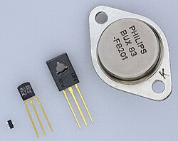
3D model of a TO-92 package, commonly used for small bipolar transistors
A bipolar junction transistor (BJT) is a type of transistor that uses both electrons and electron holes as charge carriers. In contrast, a unipolar transistor, such as a field-effect transistor (FET), uses only one kind of charge carrier. A bipolar transistor allows a small current injected at one of its terminals to control a much larger current between the remaining two terminals, making the device capable of amplification or switching.
BJTs use two p–n junctions between two semiconductor types, n-type and p-type, which are regions in a single crystal of material. The junctions can be made in several different ways, such as changing the doping of the semiconductor material as it is grown, by depositing metal pellets to form alloy junctions, or by such methods as diffusion of n-type and p-type doping substances into the crystal. The superior predictability and performance of junction transistors quickly displaced the original point-contact transistor. Diffused transistors, along with other components, are elements of integrated circuits for analog and digital functions. Hundreds of bipolar junction transistors can be made in one circuit at a very low cost.
Bipolar transistor integrated circuits were the main active devices of a generation of mainframe and minicomputers, but computer systems now use complementary metal–oxide–semiconductor (CMOS) integrated circuits relying on the field-effect transistor (FET). Bipolar transistors are still used for amplification of signals, switching, and in mixed-signal integrated circuits using BiCMOS. Specialized types are used for high voltage and high current switches, or for radio-frequency (RF) amplifiers.
Grown-junction transistor– first bipolar junction transistor made.[4] Invented by William Shockley at Bell Labs on June 23, 1948.[5] Patent filed on June 26, 1948.
Post-alloy diffused transistor (PADT)– high-speed type of alloy junction transistor, speedier than MAT, a diffused-base transistor. Developed at Philips.
Tetrode transistor– high-speed variant of grown-junction transistor[10] or alloy junction transistor[11] with two connections to base.
Drift-field transistor– high-speed bipolar junction transistor. Invented by Herbert Kroemer[14][15] at the Central Bureau of Telecommunications Technology of the German Postal Service, in 1953.
Planar transistor– the bipolar junction transistor that made mass-produced monolithic integrated circuits possible. Developed by Jean Hoerni[19] at Fairchild in 1959.
Epitaxial transistor[20]– a bipolar junction transistor made using vapor-phase deposition. See Epitaxy. Allows very precise control of doping levels and gradients.
Function
BJTs exist as PNP and NPN types, based on the doping types of the three main terminal regions. An NPN transistor comprises two semiconductor junctions that share a thin p-doped region, and a PNP transistor comprises two semiconductor junctions that share a thin n-doped region. N-type means doped with impurities (such as phosphorus or arsenic) that provide mobile electrons, while p-type means doped with impurities (such as boron) that provide holes that readily accept electrons.
NPN BJT with forward-biased B–E junction and reverse-biased B–C junction
Charge flow in a BJT is due to diffusion of charge carriers (electrons and holes) across a junction between two regions of different charge carrier concentration. The regions of a BJT are called emitter, base, and collector.[a] A discrete transistor has three leads for connection to these regions. Typically, the emitter region is heavily doped compared to the other two layers, and the collector is doped more lightly (typically ten times lighter[21]) than the base. By design, most of the BJT collector current is due to the flow of charge carriers injected from a heavily doped emitter into the base where they are minority carriers (electrons in NPNs, holes in PNPs) that diffuse toward the collector, so BJTs are classified as minority-carrier devices.
In typical operation, the base–emitter junction is forward biased, which means that the p-doped side of the junction is at a more positive potential than the n-doped side, and the base–collector junction is reverse biased. When forward bias is applied to the base–emitter junction, the equilibrium between the thermally generated carriers and the repelling electric field of the emitter depletion region is disturbed. This allows thermally excited carriers (electrons in NPNs, holes in PNPs) to inject from the emitter into the base region. These carriers create a diffusion current through the base from the region of high concentration near the emitter toward the region of low concentration near the collector.
To minimize the fraction of carriers that recombine before reaching the collector–base junction, the transistor's base region must be thin enough that carriers can diffuse across it in much less time than the semiconductor's minority-carrier lifetime. Having a lightly doped base ensures recombination rates are low. In particular, the thickness of the base must be much less than the diffusion length of the carriers. The collector–base junction is reverse-biased, and so negligible carrier injection occurs from the collector to the base, but carriers that are injected into the base from the emitter, and diffuse to reach the collector–base depletion region, are swept into the collector by the electric field in the depletion region. The thin shared base and asymmetric collector–emitter doping are what differentiates a bipolar transistor from two separate diodes connected in series.
Voltage, current, and charge control
The collector–emitter current can be viewed as being controlled by the base–emitter current (current control), or by the base–emitter voltage (voltage control). These views are related by the current–voltage relation of the base–emitter junction, which is the usual exponential current–voltage curve of a p–n junction (diode).[22]
The explanation for collector current is the concentration gradient of minority carriers in the base region.[22][23][24] Due to low-level injection (in which there are many fewer excess carriers than normal majority carriers) the ambipolar transport rates (in which the excess majority and minority carriers flow at the same rate) is in effect determined by the excess minority carriers.
Detailed transistor models of transistor action, such as the Gummel–Poon model, account for the distribution of this charge explicitly to explain transistor behavior more exactly.[25] The charge-control view easily handles phototransistors, where minority carriers in the base region are created by the absorption of photons, and handles the dynamics of turn-off, or recovery time, which depends on charge in the base region recombining. However, because base charge is not a signal that is visible at the terminals, the current- and voltage-control views are generally used in circuit design and analysis.
In analog circuit design, the current-control view is sometimes used because it is approximately linear. That is, the collector current is approximately times the base current. Some basic circuits can be designed by assuming that the base–emitter voltage is approximately constant and that collector current is β times the base current. However, to accurately and reliably design production BJT circuits, the voltage-control model (e.g. the Ebers–Moll model) is required.[22] The voltage-control model requires an exponential function to be taken into account, but when it is linearized such that the transistor can be modeled as a transconductance, as in the Ebers–Moll model, design for circuits such as differential amplifiers again becomes a mostly linear problem, so the voltage-control view is often preferred. For translinear circuits, in which the exponential I–V curve is key to the operation, the transistors are usually modeled as voltage-controlled current sources whose transconductance is proportional to their collector current. In general, transistor-level circuit analysis is performed using SPICE or a comparable analog-circuit simulator, so mathematical model complexity is usually not of much concern to the designer, but a simplified view of the characteristics allows designs to be created following a logical process.
Bipolar transistors, and particularly power transistors, have long base-storage times when they are driven into saturation; the base storage limits turn-off time in switching applications. A Baker clamp can prevent the transistor from heavily saturating, which reduces the amount of charge stored in the base and thus improves switching time.
Transistor characteristics: alpha (α) and beta (β)
The proportion of carriers able to cross the base and reach the collector is a measure of the BJT efficiency. The heavy doping of the emitter region and light doping of the base region causes many more electrons to be injected from the emitter into the base than holes to be injected from the base into the emitter. A thin and lightly doped base region means that most of the minority carriers that are injected into the base will diffuse to the collector and not recombine.
Common-emitter current gain
The common-emitter current gain is represented by βF or the h-parameterhFE; it is approximately the ratio of the collector's direct current to the base's direct current in forward-active region. (The F subscript is used to indicate the forward-active mode of operation.) It is typically greater than 50 for small-signal transistors, but can be smaller in transistors designed for high-power applications. Both injection efficiency and recombination in the base reduce the BJT gain.
Common-base current gain
Another useful characteristic is the common-base current gain, αF. The common-base current gain is approximately the gain of current from emitter to collector in the forward-active region. This ratio usually has a value close to unity; between 0.980 and 0.998. It is less than unity due to recombination of charge carriers as they cross the base region.
Alpha and beta are related by the following identities:
Beta is a convenient figure of merit to describe the performance of a bipolar transistor, but is not a fundamental physical property of the device. Bipolar transistors can be considered voltage-controlled devices (fundamentally the collector current is controlled by the base–emitter voltage; the base current could be considered a defect and is controlled by the characteristics of the base–emitter junction and recombination in the base). In many designs beta is assumed high enough so that base current has a negligible effect on the circuit. In some circuits (generally switching circuits), sufficient base current is supplied so that even the lowest beta value a particular device may have will still allow the required collector current to flow.
Structure
Simplified cross section of a planar NPN bipolar junction transistor
BJTs consists of three differently doped semiconductor regions: the emitter region, the base region and the collector region. These regions are, respectively, p type, n type and p type in a PNP transistor, and n type, p type and n type in an NPN transistor. Each semiconductor region is connected to a terminal, appropriately labeled: emitter (E), base (B) and collector (C).
The base is physically located between the emitter and the collector and is made from lightly doped, high-resistivity material. The collector surrounds the emitter region, making it almost impossible for the electrons injected into the base region to escape without being collected, thus making the resulting value of α very close to unity, and so, giving the transistor a large β. A cross-section view of a BJT indicates that the collector–base junction has a much larger area than the emitter–base junction.
The bipolar junction transistor, unlike other transistors, is usually not a symmetrical device. This means that interchanging the collector and the emitter makes the transistor leave the forward active mode and start to operate in reverse mode. Because the transistor's internal structure is usually optimized for forward-mode operation, interchanging the collector and the emitter makes the values of α and β in reverse operation much smaller than those in forward operation; often the α of the reverse mode is lower than 0.5. The lack of symmetry is primarily due to the doping ratios of the emitter and the collector. The emitter is heavily doped, while the collector is lightly doped, allowing a large reverse bias voltage to be applied before the collector–base junction breaks down. The collector–base junction is reverse biased in normal operation. The reason the emitter is heavily doped is to increase the emitter injection efficiency: the ratio of carriers injected by the emitter to those injected by the base. For high current gain, most of the carriers injected into the emitter–base junction must come from the emitter.
Die of a 2N2222 NPN transistor: the NPN materials are made in layers with the collector at the bottom. Bond wires connect metalization on the base to the left lead, and emitter to the right. The collector is connected to the can with a third external lead.
The low-performance "lateral" bipolar transistors sometimes used in bipolar and MOS integrated circuits are sometimes designed symmetrically, that is, with no difference between forward and backward operation.
Small changes in the voltage applied across the base–emitter terminals cause the current between the emitter and the collector to change significantly. This effect can be used to amplify the input voltage or current. BJTs can be thought of as voltage-controlled current sources, but are more simply characterized as current-controlled current sources, or current amplifiers, due to the low impedance at the base.
Early transistors were made from germanium but most modern BJTs are made from silicon. A significant minority are also now made from gallium arsenide, especially for very high speed applications (see HBT, below).
The heterojunction bipolar transistor (HBT) is an improvement of the BJT that can handle signals of very high frequencies up to several hundred GHz. It is common in modern ultrafast circuits, mostly RF systems.[26][27]
Symbol for NPN bipolar transistor with current flow direction
Two commonly used HBTs are silicon–germanium and aluminum gallium arsenide, though a wide variety of semiconductors may be used for the HBT structure. HBT structures are usually grown by epitaxy techniques like MOCVD and MBE.
Regions of operation
Junction type
Applied voltages
Junction bias
Mode
B–E
B–C
NPN
E < B < C
Forward
Reverse
Forward-active
E < B > C
Forward
Forward
Saturation
E > B < C
Reverse
Reverse
Cut-off
E > B > C
Reverse
Forward
Reverse-active
PNP
E < B < C
Reverse
Forward
Reverse-active
E < B > C
Reverse
Reverse
Cut-off
E > B < C
Forward
Forward
Saturation
E > B > C
Forward
Reverse
Forward-active
Bipolar transistors have four distinct regions of operation, defined by BJT junction biases:[28][29]
Forward-active (or simply active)
The base–emitter junction is forward biased and the base–collector junction is reverse biased. Most bipolar transistors are designed to afford the greatest common-emitter current gain, βF, in forward-active mode. If this is the case, the collector–emitter current is approximately proportional to the base current, but many times larger, for small base current variations.
Reverse-active (or inverse-active or inverted)
By reversing the biasing conditions of the forward-active region, a bipolar transistor goes into reverse-active mode. In this mode, the emitter and collector regions switch roles. Because most BJTs are designed to maximize current gain in forward-active mode, the βF in inverted mode is several times smaller (2–3 times for the ordinary germanium transistor). This transistor mode is seldom used, usually being considered only for failsafe conditions and some types of bipolar logic. The reverse bias breakdown voltage to the base may be an order of magnitude lower in this region.
Saturation
With both junctions forward biased, a BJT is in saturation mode and facilitates high current conduction from the emitter to the collector (or the other direction in the case of NPN, with negatively charged carriers flowing from emitter to collector). This mode corresponds to a logical "on", or a closed switch.
Cut-off
In cut-off, biasing conditions opposite of saturation (both junctions reverse biased) are present. There is very little current, which corresponds to a logical "off", or an open switch.
Input characteristics
Output characteristics
Input and output characteristics for a common-base silicon transistor amplifier.
Although these regions are well defined for sufficiently large applied voltage, they overlap somewhat for small (less than a few hundred millivolts) biases. For example, in the typical grounded-emitter configuration of an NPN BJT used as a pulldown switch in digital logic, the "off" state never involves a reverse-biased junction because the base voltage never goes below ground; nevertheless the forward bias is close enough to zero that essentially no current flows, so this end of the forward active region can be regarded as the cutoff region.
Active-mode transistors in circuits
Structure and use of NPN transistor; arrow according to schematic
The diagram shows a schematic representation of an NPN transistor connected to two voltage sources. (The same description applies to a PNP transistor with reversed directions of current flow and applied voltage.) This applied voltage causes the lower p–n junction to become forward biased, allowing a flow of electrons from the emitter into the base. In active mode, the electric field existing between base and collector (caused by VCE) will cause the majority of these electrons to cross the upper p–n junction into the collector to form the collector current IC. The remainder of the electrons recombine with holes, the majority carriers in the base, making a current through the base connection to form the base current, IB. As shown in the diagram, the emitter current, IE, is the total transistor current, which is the sum of the other terminal currents, (i.e. IE=IB+IC).
In the diagram, the arrows representing current point in the direction of conventional current– the flow of electrons is in the opposite direction of the arrows because electrons carry negative electric charge. In active mode, the ratio of the collector current to the base current is called the DC current gain. This gain is usually 100 or more, but robust circuit designs do not depend on the exact value (for example see op-amp). The value of this gain for DC signals is referred to as , and the value of this gain for small signals is referred to as . That is, when a small change in the currents occurs, and sufficient time has passed for the new condition to reach a steady state is the ratio of the change in collector current to the change in base current. The symbol is used for both and .[22]:62–66
The emitter current is related to exponentially. At room temperature, an increase in by approximately 60mV increases the emitter current by a factor of 10. Because the base current is approximately proportional to the collector and emitter currents, they vary in the same way.
Theory and modeling
Band diagram for NPN transistor at equilibriumBand diagram for NPN transistor in active mode, showing injection of electrons from emitter to base, and their overshoot into the collector
BJTs can be thought of as two diodes (p–n junctions) sharing a common region that minority carriers can move through. A PNP BJT will function like two diodes that share an N-type cathode region, and the NPN like two diodes sharing a P-type anode region. Connecting two diodes with wires will not make a BJT, since minority carriers will not be able to get from one p–n junction to the other through the wire.
Both types of BJT function by letting a small current input to the base control an amplified output from the collector. The result is that the BJT makes a good switch that is controlled by its base input. The BJT also makes a good amplifier, since it can multiply a weak input signal to about 100 times its original strength. Networks of BJTs are used to make powerful amplifiers with many different applications.
In the discussion below, focus is on the NPN BJT. In what is called active mode, the base–emitter voltage and collector–base voltage are positive, forward biasing the emitter–base junction and reverse-biasing the collector–base junction. In this mode, electrons are injected from the forward biased n-type emitter region into the p-type base where they diffuse as minority carriers to the reverse-biased n-type collector and are swept away by the electric field in the reverse-biased collector–base junction.
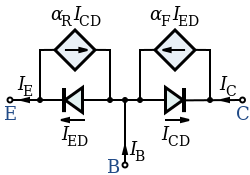
Ebers–Moll model for an NPN transistor. IB, IC and IE are the base, collector and emitter currents; ICD and IED are the collector and emitter diode currents; αF and αR are the forward and reverse common-base current gains.Ebers–Moll model for a PNP transistorApproximated Ebers–Moll model for an NPN transistor in the forward active mode. The collector diode is reverse-biased so ICD is virtually zero. Most of the emitter diode current (αF is nearly 1) is drawn from the collector, providing the amplification of the base current.
The DC emitter and collector currents in active mode are well modeled by an approximation to the Ebers–Moll model:
The base internal current is mainly by diffusion (see Fick's law) and
where
is the thermal voltage (approximately 26mV at 300K ≈ room temperature).
is the emitter current
is the collector current
is the common base forward short-circuit current gain (0.98 to 0.998)
is the reverse saturation current of the base–emitter diode (on the order of 10−15 to 10−12 amperes)
is the base–emitter voltage
is the diffusion constant for electrons in the p-type base
W is the base width
The and forward parameters are as described previously. A reverse is sometimes included in the model.
The unapproximated Ebers–Moll equations used to describe the three currents in any operating region are given below. These equations are based on the transport model for a bipolar junction transistor.[32]
where
is the collector current
is the base current
is the emitter current
is the forward common emitter current gain (20 to 500)
is the reverse common emitter current gain (0 to 20)
is the reverse saturation current (on the order of 10−15 to 10−12 amperes)
is the thermal voltage (approximately 26mV at 300 K ≈ room temperature).
Top: NPN base width for low collector–base reverse bias; Bottom: narrower NPN base width for large collector–base reverse bias. Hashed regions are depleted regions.
As the collector–base voltage () varies, the collector–base depletion region varies in size. An increase in the collector–base voltage, for example, causes a greater reverse bias across the collector–base junction, increasing the collector–base depletion region width, and decreasing the width of the base. This variation in base width often is called the Early effect after its discoverer James M. Early.
Narrowing of the base width has two consequences:
There is a lesser chance for recombination within the "smaller" base region.
The charge gradient is increased across the base, and consequently, the current of minority carriers injected across the emitter junction increases.
Both factors increase the collector or "output" current of the transistor in response to an increase in the collector–base voltage.
Punchthrough
When the base–collector voltage reaches a certain (device-specific) value, the base–collector depletion region boundary meets the base–emitter depletion region boundary. When in this state the transistor effectively has no base. The device thus loses all gain when in this state.
Gummel–Poon charge-control model
The Gummel–Poon model[33] is a detailed charge-controlled model of BJT dynamics, which has been adopted and elaborated by others to explain transistor dynamics in greater detail than the terminal-based models typically do.[34] This model also includes the dependence of transistor -values upon the direct current levels in the transistor, which are assumed current-independent in the Ebers–Moll model.[35]
The hybrid-pi model is a popular circuit model used for analyzing the small signal and AC behavior of bipolar junction and field effect transistors. Sometimes it is also called Giacoletto model because it was introduced by L.J. Giacoletto in 1969. The model can be quite accurate for low-frequency circuits and can easily be adapted for higher-frequency circuits with the addition of appropriate inter-electrode capacitances and other parasitic elements.
h-parameter model
Generalized h-parameter model of an NPN BJT. Replace x with e, b or c for CE, CB and CC topologies respectively.
Another model commonly used to analyze BJT circuits is the h-parameter model, also known as the hybrid equivalent model, closely related to the hybrid-pi model and the y-parametertwo-port, but using input current and output voltage as independent variables, rather than input and output voltages. This two-port network is particularly suited to BJTs as it lends itself easily to the analysis of circuit behavior, and may be used to develop further accurate models. As shown, the term x in the model represents a different BJT lead depending on the topology used. For common-emitter mode the various symbols take on the specific values as:
Terminal 1, base
Terminal 2, collector
Terminal 3 (common), emitter; giving x to be e
ii, base current (ib)
io, collector current (ic)
Vin, base-to-emitter voltage (VBE)
Vo, collector-to-emitter voltage (VCE)
and the h-parameters are given by:
hix = hie for the common-emitter configuration, the input impedance of the transistor (corresponding to the base resistance rpi).
hrx = hre, a reverse transfer relationship, it represents the dependence of the transistor's (input) IB–VBE curve on the value of (output) VCE. It is usually very small and is often neglected (assumed to be zero) at DC.
hfx = hfe, the "forward" current-gain of the transistor, sometimes written h21. This parameter, with lower case "fe" to imply small signal (AC) gain, or more often with capital letters for "FE" (specified as hFE) to mean the "large signal" or DC current-gain (βDC or often simply β), is one of the main parameters in datasheets, and may be given for a typical collector current and voltage or plotted as a function of collector current. See below.
hox = 1/hoe, the output impedance of transistor. The parameter hoe usually corresponds to the output admittance of the bipolar transistor and has to be inverted to convert it to an impedance.
As shown, the h-parameters have lower-case subscripts and hence signify AC conditions or analyses. For DC conditions they are specified in upper-case. For the CE topology, an approximate h-parameter model is commonly used which further simplifies the circuit analysis. For this the hoe and hre parameters are neglected (that is, they are set to infinity and zero, respectively). The h-parameter model as shown is suited to low-frequency, small-signal analysis. For high-frequency analyses the inter-electrode capacitances that are important at high frequencies must be added.
Etymology of hFE
The h refers to its being an h-parameter, a set of parameters named for their origin in a hybrid equivalent circuit model (see above). As with all h parameters, the choice of lower case or capitals for the letters that follow the "h" is significant; lower-case signifies "small signal" parameters, that is, the slope the particular relationship; upper-case letters imply "large signal" or DC values, the ratio of the voltages or currents. In the case of the very often used hFE:
F is from Forward current amplification also called the current gain.
E refers to the transistor operating in a common Emitter (CE) configuration.
So hFE (or hFE) refers to the (total; DC) collector current divided by the base current, and is dimensionless. It is a parameter that varies somewhat with collector current, but is often approximated as a constant; it is normally specified at a typical collector current and voltage, or graphed as a function of collector current.
Had capital letters not been used for used in the subscript, i.e. if it were written hfe the parameter indicate small signal (AC) current gain, i.e. the slope of the Collector current versus Base current graph at a given point, which is often close to the hFE value unless the test frequency is high.
The Gummel–Poon SPICE model is often used, but it suffers from several limitations. For instance, reverse breakdown of the base–emitter diode is not captured by the SGP (SPICE Gummel–Poon) model, neither are thermal effects (self-heating) or quasi-saturation.[36] These have been addressed in various more advanced models which either focus on specific cases of application (Mextram, HICUM, Modella) or are designed for universal usage (VBIC).[37][38][39][40]
Current direction conventions
By convention, the direction of current on diagrams is shown as the direction in which a positive charge would move. This is called conventional current. However, in actuality, current in metal conductors is[b] due to the flow of electrons. Because electrons carry a negative charge, they move in the direction opposite to conventional current. On the other hand, inside a bipolar transistor, currents can be composed of both positively charged holes and negatively charged electrons. In this article, current arrows are shown in the conventional direction, but labels for the movement of holes and electrons show their actual direction inside the transistor.
Arrow direction
The arrow on the symbol for bipolar transistors indicates the p–n junction between base and emitter and points in the direction in which conventional current travels.
Applications
The BJT remains a device that excels in some applications, such as discrete circuit design, due to the very wide selection of BJT types available, and because of its high transconductance and output resistance compared to MOSFETs.
The BJT is also the choice for demanding analog circuits, especially for very-high-frequency applications, such as radio-frequency circuits for wireless systems.
Bipolar transistors can be combined with MOSFETs in an integrated circuit by using a BiCMOS process of wafer fabrication to create circuits that take advantage of the application strengths of both types of transistor.
One of the most prominent early uses of the transistor was in consumer products such as the transistor radio which began production in 1954. The use of transistors in handheld radios and would also jumpstart a small Japanese company named Tokyo Tsushin Kogyo K.K. to prominence with its TR-55 transistor radio bearing the name the company would soon change to match: Sony. The follow-on pocket-sized Sony TR-63 and several larger models by other manufacturers cemented the transistor and miniaturized electronics as critical to the new, portable consumer device market for decades to come.[citation needed]
The transistor parameters α and β characterize the current gain of the BJT. It is this gain that allows BJTs to be used as the building blocks of electronic amplifiers. The three main BJT amplifier topologies are:
Because of the known temperature and current dependence of the forward-biased base–emitter junction voltage, the BJT can be used to measure temperature by subtracting two voltages at two different bias currents in a known ratio.[42]
Logarithmic converters
Because base–emitter voltage varies as the logarithm of the base–emitter and collector–emitter currents, a BJT can also be used to compute logarithms and anti-logarithms. A diode can also perform these nonlinear functions but the transistor provides more circuit flexibility.
Avalanche pulse generators
Transistors may be deliberately made with a lower collector to emitter breakdown voltage than the collector to base breakdown voltage. If the emitter–base junction is reverse biased the collector emitter voltage may be maintained at a voltage just below breakdown. As soon as the base voltage is allowed to rise, and current flows avalanche occurs and impact ionization in the collector base depletion region rapidly floods the base with carriers and turns the transistor fully on. So long as the pulses are short enough and infrequent enough that the device is not damaged, this effect can be used to create very sharp falling edges.
↑Morris, Peter Robin (1990). "4.2". A History of the World Semiconductor Industry. IEE History of Technology Series 12. London: Peter Peregrinus Ltd. p.29. ISBN978-0-86341-227-1.
↑Brar, B.; Sullivan, G.J.; Asbeck, P.M. (2001). "Herb's bipolar transistors". IEEE Transactions on Electron Devices. 48 (11): 2473–2476. Bibcode:2001ITED...48.2473B. doi:10.1109/16.960370.
↑Bullis, W.M.; Runyan, W.R. (1967). "Influence of mobility and lifetime variations on drift-field effects in silicon-junction devices". IEEE Transactions on Electron Devices. 14 (2): 75–81. Bibcode:1967ITED...14...75B. doi:10.1109/T-ED.1967.15902.
↑General Electric (1962). Transistor Manual (6thed.). p.12. Bibcode:1964trma.book.....C. "If the principle of space charge neutrality is used in the analysis of the transistor, it is evident that the collector current is controlled by means of the positive charge (hole concentration) in the base region. ... When a transistor is used at higher frequencies, the fundamental limitation is the time it takes the carriers to diffuse across the base region..." (same in 4th and 5th editions).
This page is based on this Wikipedia article Text is available under the CC BY-SA 4.0 license; additional terms may apply. Images, videos and audio are available under their respective licenses.