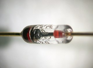
A diode is a two-terminal electronic component that conducts current primarily in one direction. It has low resistance in one direction and high resistance in the other.
A PIN diode is a diode with a wide, undoped intrinsic semiconductor region between a p-type semiconductor and an n-type semiconductor region. The p-type and n-type regions are typically heavily doped because they are used for ohmic contacts.

A bipolar junction transistor (BJT) is a type of transistor that uses both electrons and electron holes as charge carriers. In contrast, a unipolar transistor, such as a field-effect transistor (FET), uses only one kind of charge carrier. A bipolar transistor allows a small current injected at one of its terminals to control a much larger current between the remaining two terminals, making the device capable of amplification or switching.

A Zener diode is a special type of diode designed to reliably allow current to flow "backwards" when a certain set reverse voltage, known as the Zener voltage, is reached.
A thyristor is a solid-state semiconductor device which can be thought of as being a highly robust and switchable diode, allowing the passage of current in one direction but not the other, often under control of a gate electrode, that is used in high power applications like inverters and radar generators. It usually consists of four layers of alternating P- and N-type materials. It acts as a bistable switch. There are two designs, differing in what triggers the conducting state. In a three-lead thyristor, a small current on its gate lead controls the larger current of the anode-to-cathode path. In a two-lead thyristor, conduction begins when the potential difference between the anode and cathode themselves is sufficiently large. The thyristor continues conducting until the voltage across the device is reverse-biased or the voltage is removed, or through the control gate signal on newer types.

The Schottky diode, also known as Schottky barrier diode or hot-carrier diode, is a semiconductor diode formed by the junction of a semiconductor with a metal. It has a low forward voltage drop and a very fast switching action. The cat's-whisker detectors used in the early days of wireless and metal rectifiers used in early power applications can be considered primitive Schottky diodes.

In electronics, a varicap diode, varactor diode, variable capacitance diode, variable reactance diode or tuning diode is a type of diode designed to exploit the voltage-dependent capacitance of a reverse-biased p–n junction.

A silicon controlled rectifier or semiconductor controlled rectifier is a four-layer solid-state current-controlling device. The name "silicon controlled rectifier" is General Electric's trade name for a type of thyristor. The principle of four-layer p–n–p–n switching was developed by Moll, Tanenbaum, Goldey, and Holonyak of Bell Laboratories in 1956. The practical demonstration of silicon controlled switching and detailed theoretical behavior of a device in agreement with the experimental results was presented by Dr Ian M. Mackintosh of Bell Laboratories in January 1958. The SCR was developed by a team of power engineers led by Gordon Hall and commercialized by Frank W. "Bill" Gutzwiller in 1957.
A TRIAC is a three-terminal electronic component that conducts current in either direction when triggered. The term TRIAC is a genericised trademark.

A Schottky barrier, named after Walter H. Schottky, is a potential energy barrier for electrons formed at a metal–semiconductor junction. Schottky barriers have rectifying characteristics, suitable for use as a diode. One of the primary characteristics of a Schottky barrier is the Schottky barrier height, denoted by ΦB. The value of ΦB depends on the combination of metal and semiconductor.

A tunnel diode or Esaki diode is a type of semiconductor diode that has effectively "negative resistance" due to the quantum mechanical effect called tunneling. It was invented in August 1957 by Leo Esaki and Yuriko Kurose when working at Tokyo Tsushin Kogyo, now known as Sony. In 1973, Esaki received the Nobel Prize in Physics for experimental demonstration of the electron tunneling effect in semiconductors. Robert Noyce independently devised the idea of a tunnel diode while working for William Shockley, but was discouraged from pursuing it. Tunnel diodes were first manufactured by Sony in 1957, followed by General Electric and other companies from about 1960, and are still made in low volume today.

A p–n junction is a combination of two types of semiconductor materials, p-type and n-type, in a single crystal. The "n" (negative) side contains freely-moving electrons, while the "p" (positive) side contains freely-moving electron holes. Connecting the two materials causes creation of a depletion region near the boundary, as the free electrons fill the available holes, which in turn allows electric current to pass through the junction only in one direction.
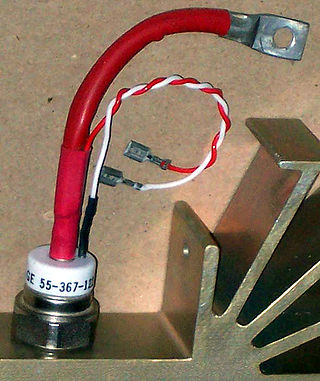
A power semiconductor device is a semiconductor device used as a switch or rectifier in power electronics. Such a device is also called a power device or, when used in an integrated circuit, a power IC.

A single-photon avalanche diode (SPAD), also called Geiger-mode avalanche photodiode is a solid-state photodetector within the same family as photodiodes and avalanche photodiodes (APDs), while also being fundamentally linked with basic diode behaviours. As with photodiodes and APDs, a SPAD is based around a semi-conductor p-n junction that can be illuminated with ionizing radiation such as gamma, x-rays, beta and alpha particles along with a wide portion of the electromagnetic spectrum from ultraviolet (UV) through the visible wavelengths and into the infrared (IR).
Diffusion Capacitance is the capacitance that happens due to transport of charge carriers between two terminals of a device, for example, the diffusion of carriers from anode to cathode in a forward biased diode or from emitter to base in a forward-biased junction of a transistor. In a semiconductor device with a current flowing through it at a particular moment there is necessarily some charge in the process of transit through the device. If the applied voltage changes to a different value and the current changes to a different value, a different amount of charge will be in transit in the new circumstances. The change in the amount of transiting charge divided by the change in the voltage causing it is the diffusion capacitance. The adjective "diffusion" is used because the original use of this term was for junction diodes, where the charge transport was via the diffusion mechanism. See Fick's laws of diffusion.
The saturation current, more accurately the reverse saturation current, is the part of the reverse current in a semiconductor diode caused by diffusion of minority carriers from the neutral regions to the depletion region. This current is almost independent of the reverse voltage.
In semiconductor physics, the depletion region, also called depletion layer, depletion zone, junction region, space charge region, or space charge layer, is an insulating region within a conductive, doped semiconductor material where the mobile charge carriers have diffused away, or been forced away by an electric field. The only elements left in the depletion region are ionized donor or acceptor impurities. This region of uncovered positive and negative ions is called the depletion region due to the depletion of carriers in this region, leaving none to carry a current. Understanding the depletion region is key to explaining modern semiconductor electronics: diodes, bipolar junction transistors, field-effect transistors, and variable capacitance diodes all rely on depletion region phenomena.
A noise-figure meter is an instrument for measuring the noise figure of an amplifier, mixer, or similar device. An example instrument is the 1983-era Agilent 8970A. The 8970A Noise Figure Meter is a Keysight product numbers that were formerly part of Agilent.

A noise generator is a circuit that produces electrical noise. Noise generators are used to test signals for measuring noise figure, frequency response, and other parameters. Noise generators are also used for generating random numbers.
A p–n diode is a type of semiconductor diode based upon the p–n junction. The diode conducts current in only one direction, and it is made by joining a p-type semiconducting layer to an n-type semiconducting layer. Semiconductor diodes have multiple uses including rectification of alternating current to direct current, in the detection of radio signals, and emitting and detecting light.
The following two books contain a comprehensive analysis of the theory of non-equilibrium charge transport in semiconductor diodes, and give also an overview of applications (at least up to the end of the seventies).
The following application notes deals extensively with practical circuits and applications using SRDs.


