
Organic electronics is a field of materials science concerning the design, synthesis, characterization, and application of organic molecules or polymers that show desirable electronic properties such as conductivity. Unlike conventional inorganic conductors and semiconductors, organic electronic materials are constructed from organic (carbon-based) molecules or polymers using synthetic strategies developed in the context of organic chemistry and polymer chemistry.
A semiconductor material has an electrical conductivity value falling between that of a conductor, such as metallic copper, and an insulator, such as glass. Its resistivity falls as its temperature rises; metals behave in the opposite way. Its conducting properties may be altered in useful ways by introducing impurities ("doping") into the crystal structure. When two differently-doped regions exist in the same crystal, a semiconductor junction is created. The behavior of charge carriers, which include electrons, ions and electron holes, at these junctions is the basis of diodes, transistors and most modern electronics. Some examples of semiconductors are silicon, germanium, gallium arsenide, and elements near the so-called "metalloid staircase" on the periodic table. After silicon, gallium arsenide is the second most common semiconductor and is used in laser diodes, solar cells, microwave-frequency integrated circuits, and others. Silicon is a critical element for fabricating most electronic circuits.
A semiconductor device is an electronic component that relies on the electronic properties of a semiconductor material for its function. Semiconductor devices have replaced vacuum tubes in most applications. They use electrical conduction in the solid state rather than the gaseous state or thermionic emission in a vacuum.
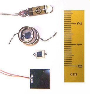
A photodiode is a semiconductor p-n junction device that converts light into an electrical current. The current is generated when photons are absorbed in the photodiode. Photodiodes may contain optical filters, built-in lenses, and may have large or small surface areas. Photodiodes usually have a slower response time as their surface area increases. The common, traditional solar cell used to generate electric solar power is a large area photodiode.
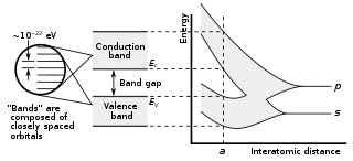
In solid-state physics, a band gap, also called an energy gap, is an energy range in a solid where no electronic states can exist. In graphs of the electronic band structure of solids, the band gap generally refers to the energy difference between the top of the valence band and the bottom of the conduction band in insulators and semiconductors. It is the energy required to promote a valence electron bound to an atom to become a conduction electron, which is free to move within the crystal lattice and serve as a charge carrier to conduct electric current. It is closely related to the HOMO/LUMO gap in chemistry. If the valence band is completely full and the conduction band is completely empty, then electrons cannot move in the solid; however, if some electrons transfer from the valence to the conduction band, then current can flow. Therefore, the band gap is a major factor determining the electrical conductivity of a solid. Substances with large band gaps are generally insulators, those with smaller band gaps are semiconductors, while conductors either have very small band gaps or none, because the valence and conduction bands overlap.
Organic semiconductors are solids whose building blocks are pi-bonded molecules or polymers made up by carbon and hydrogen atoms and – at times – heteroatoms such as nitrogen, sulfur and oxygen. They exist in form of molecular crystals or amorphous thin films. In general, they are electrical insulators, but become semiconducting when charges are either injected from appropriate electrodes, upon doping or by photoexcitation.
A "photoelectrochemical cell" is one of two distinct classes of device. The first produces electrical energy similarly to a dye-sensitized photovoltaic cell, which meets the standard definition of a photovoltaic cell. The second is a photoelectrolytic cell, that is, a device which uses light incident on a photosensitizer, semiconductor, or aqueous metal immersed in an electrolytic solution to directly cause a chemical reaction, for example to produce hydrogen via the electrolysis of water.

The term quantum efficiency (QE) may apply to incident photon to converted electron (IPCE) ratio of a photosensitive device, or it may refer to the TMR effect of a Magnetic Tunnel Junction.

Photodetectors, also called photosensors, are sensors of light or other electromagnetic radiation. There is a wide variety of photodetectors which may be classified by mechanism of detection, such as photoelectric or photochemical effects, or by various performance metrics, such as spectral response. Semiconductor-based photodetectors typically have a p–n junction that converts light photons into current. The absorbed photons make electron–hole pairs in the depletion region. Photodiodes and phototransistors are a few examples of photodetectors. Solar cells convert some of the light energy absorbed into electrical energy.

A dye-sensitized solar cell is a low-cost solar cell belonging to the group of thin film solar cells. It is based on a semiconductor formed between a photo-sensitized anode and an electrolyte, a photoelectrochemical system. The modern version of a dye solar cell, also known as the Grätzel cell, was originally co-invented in 1988 by Brian O'Regan and Michael Grätzel at UC Berkeley and this work was later developed by the aforementioned scientists at the École Polytechnique Fédérale de Lausanne (EPFL) until the publication of the first high efficiency DSSC in 1991. Michael Grätzel has been awarded the 2010 Millennium Technology Prize for this invention.
The photovoltaic effect is the generation of voltage and electric current in a material upon exposure to light. It is a physical and chemical phenomenon.
Hybrid solar cells combine advantages of both organic and inorganic semiconductors. Hybrid photovoltaics have organic materials that consist of conjugated polymers that absorb light as the donor and transport holes. Inorganic materials in hybrid cells are used as the acceptor and electron transporter in the structure. The hybrid photovoltaic devices have a potential for not only low-cost by roll-to-roll processing but also for scalable solar power conversion.

A quantum dot solar cell (QDSC) is a solar cell design that uses quantum dots as the absorbing photovoltaic material. It attempts to replace bulk materials such as silicon, copper indium gallium selenide (CIGS) or cadmium telluride (CdTe). Quantum dots have bandgaps that are tunable across a wide range of energy levels by changing their size. In bulk materials, the bandgap is fixed by the choice of material(s). This property makes quantum dots attractive for multi-junction solar cells, where a variety of materials are used to improve efficiency by harvesting multiple portions of the solar spectrum.
The anomalous photovoltaic effect (APE), also called the bulk photovoltaic effect in certain cases, is a type of a photovoltaic effect which occurs in certain semiconductors and insulators. The "anomalous" refers to those cases where the photovoltage is larger than the band gap of the corresponding semiconductor. In some cases, the voltage may reach thousands of volts.
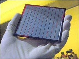
Organic photovoltaic devices (OPVs) are fabricated from thin films of organic semiconductors, such as polymers and small-molecule compounds, and are typically on the order of 100 nm thick. Because polymer based OPVs can be made using a coating process such as spin coating or inkjet printing, they are an attractive option for inexpensively covering large areas as well as flexible plastic surfaces. A promising low cost alternative to conventional solar cells made of crystalline silicon, there is a large amount of research being dedicated throughout industry and academia towards developing OPVs and increasing their power conversion efficiency.
An organic solar cell (OSC) or plastic solar cell is a type of photovoltaic that uses organic electronics, a branch of electronics that deals with conductive organic polymers or small organic molecules, for light absorption and charge transport to produce electricity from sunlight by the photovoltaic effect. Most organic photovoltaic cells are polymer solar cells.
A plasmonic-enhanced solar cell, commonly referred to simply as plasmonic solar cell, is a type of solar cell that converts light into electricity with the assistance of plasmons, but where the photovoltaic effect occurs in another material.
Two-photon photovoltaic effect is an energy collection method based on two-photon absorption (TPA). The TPP effect can be thought of as the nonlinear equivalent of the traditional photovoltaic effect involving high optical intensities. This effect occurs when two photons are absorbed at the same time resulting in an electron-hole pair.

The field-effect transistor (FET) is a type of transistor that uses an electric field to control the flow of current. FETs are devices with three terminals: source, gate, and drain. FETs control the flow of current by the application of a voltage to the gate, which in turn alters the conductivity between the drain and source.

Amorphous silicon (a-Si) is the non-crystalline form of silicon used for solar cells and thin-film transistors in LCDs.

