Semiconductor devices are manufactured both as single discrete devices and as integrated circuits, which consist of two or more devices—which can number from the hundreds to the billions—manufactured and interconnected on a single semiconductor wafer (also called a substrate).
Semiconductor materials are useful because their behavior can be easily manipulated by the deliberate addition of impurities, known as doping. Semiconductor conductivity can be controlled by the introduction of an electric or magnetic field, by exposure to light or heat, or by the mechanical deformation of a doped monocrystalline silicon grid; thus, semiconductors can make excellent sensors. Current conduction in a semiconductor occurs due to mobile or "free" electrons and electron holes, collectively known as charge carriers. Doping a semiconductor with a small proportion of an atomic impurity, such as phosphorus or boron, greatly increases the number of free electrons or holes within the semiconductor. When a doped semiconductor contains excess holes, it is called a p-type semiconductor (p for positive electric charge); when it contains excess free electrons, it is called an n-type semiconductor (n for a negative electric charge). A majority of mobile charge carriers have negative charges. The manufacture of semiconductors controls precisely the location and concentration of p- and n-type dopants. The connection of n-type and p-type semiconductors form p–n junctions.
The most common semiconductor device in the world is the MOSFET (metal–oxide–semiconductor field-effect transistor),[1] also called the MOS transistor. As of 2013, billions of MOS transistors are manufactured every day.[2] Semiconductor devices made per year have been growing by 9.1% on average since 1978, and shipments in 2018 are predicted for the first time to exceed 1 trillion,[3] meaning that well over 7 trillion have been made to date.
A semiconductor diode is a device typically made from a single p–n junction. At the junction of a p-type and an n-type semiconductor, there forms a depletion region where current conduction is inhibited by the lack of mobile charge carriers. When the device is forward biased (connected with the p-side, having a higher electric potential than the n-side), this depletion region is diminished, allowing for significant conduction. Contrariwise, only a very small current can be achieved when the diode is reverse biased (connected with the n-side at higher electric potential than the p-side, and thus the depletion region expanded).
Bipolar junction transistors (BJTs) are formed from two p–n junctions, in either n–p–n or p–n–p configuration. The middle, or base, the region between the junctions is typically very narrow. The other regions, and their associated terminals, are known as the emitter and the collector. A small current injected through the junction between the base and the emitter changes the properties of the base-collector junction so that it can conduct current even though it is reverse biased. This creates a much larger current between the collector and emitter, controlled by the base-emitter current.
Another type of transistor, the field-effect transistor (FET), operates on the principle that semiconductor conductivity can be increased or decreased by the presence of an electric field. An electric field can increase the number of free electrons and holes in a semiconductor, thereby changing its conductivity. The field may be applied by a reverse-biased p–n junction, forming a junction field-effect transistor (JFET) or by an electrode insulated from the bulk material by an oxide layer, forming a metal–oxide–semiconductor field-effect transistor (MOSFET).
Operation of a MOSFET and its Id-Vg curve. At first, when no gate voltage is applied, there is no inversion electron in the channel and the device is OFF. As gate voltage increase, the inversion electron density in the channel increase, the current increases, until the device turns ON.
The metal-oxide-semiconductor FET (MOSFET, or MOS transistor), a solid-state device, is by far the most used widely semiconductor device today. It accounts for at least 99.9% of all transistors, and there have been an estimated 13sextillion MOSFETs manufactured between 1960 and 2018.[4]
The gate electrode is charged to produce an electric field that controls the conductivity of a "channel" between two terminals, called the source and drain. Depending on the type of carrier in the channel, the device may be an n-channel (for electrons) or a p-channel (for holes) MOSFET. Although the MOSFET is named in part for its "metal" gate, in modern devices polysilicon is typically used instead.
By far, silicon (Si) is the most widely used material in semiconductor devices. Its combination of low raw material cost, relatively simple processing, and a useful temperature range makes it currently the best compromise among the various competing materials. Silicon used in semiconductor device manufacturing is currently fabricated into boules that are large enough in diameter to allow the production of 300mm (12 in.) wafers.
Germanium (Ge) was a widely used early semiconductor material but its thermal sensitivity makes it less useful than silicon. Today, germanium is often alloyed with silicon for use in very-high-speed SiGe devices; IBM is a major producer of such devices.
Gallium arsenide (GaAs) is also widely used in high-speed devices but so far, it has been difficult to form large-diameter boules of this material, limiting the wafer diameter to sizes significantly smaller than silicon wafers thus making mass production of GaAs devices significantly more expensive than silicon.
Gallium Nitride (GaN) is gaining popularity in high-power applications including power ICs, light-emitting diodes (LEDs), and RF components due to its high strength and thermal conductivity. Compared to silicon, GaN's band gap is more than 3 times wider at 3.4 eV and it conducts electrons 1,000 times more efficiently.[5][6]
Other less common materials are also in use or under investigation.
Silicon carbide (SiC) is also gaining popularity in power ICs and has found some application as the raw material for blue LEDs and is being investigated for use in semiconductor devices that could withstand very high operating temperatures and environments with the presence of significant levels of ionizing radiation. IMPATT diodes have also been fabricated from SiC.
All transistor types can be used as the building blocks of logic gates, which are fundamental in the design of digital circuits. In digital circuits like microprocessors, transistors act as on-off switches; in the MOSFET, for instance, the voltage applied to the gate determines whether the switch is on or off.
Transistors used for analog circuits do not act as on-off switches; rather, they respond to a continuous range of inputs with a continuous range of outputs. Common analog circuits include amplifiers and oscillators.
Circuits that interface or translate between digital circuits and analog circuits are known as mixed-signal circuits.
Power semiconductor devices are discrete devices or integrated circuits intended for high current or high voltage applications. Power integrated circuits combine IC technology with power semiconductor technology, these are sometimes referred to as "smart" power devices. Several companies specialize in manufacturing power semiconductors.
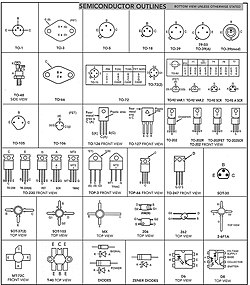
Component identifiers
The part numbers of semiconductor devices are often manufacturer specific. Nevertheless, there have been attempts at creating standards for type codes, and a subset of devices follow those. For discrete devices, for example, there are three standards: JEDEC JESD370B in the United States, Pro Electron in Europe, and Japanese Industrial Standards (JIS).
The fabrication process is performed in highly specialized semiconductor fabrication plants, also called foundries or "fabs",[8] with the central part being the "clean room". In more advanced semiconductor devices, such as modern 14/10/7nm nodes, fabrication can take up to 15 weeks, with 11–13 weeks being the industry average.[9] Production in advanced fabrication facilities is completely automated, with automated material handling systems taking care of the transport of wafers from machine to machine.[10]
A wafer often has several integrated circuits, which are called dies as they are pieces diced from a single wafer. Individual dies are separated from a finished wafer in a process called die singulation, also called wafer dicing. The dies can then undergo further assembly and packaging.[11]
Within fabrication plants, the wafers are transported inside special sealed plastic boxes called FOUPs.[10] FOUPs in many fabs contain an internal nitrogen atmosphere[12][13] which helps prevent copper from oxidizing on the wafers. Copper is used in modern semiconductors for wiring.[14] The insides of the processing equipment and FOUPs is kept cleaner than the surrounding air in the cleanroom. This internal atmosphere is known as a mini-environment and helps improve yield, which is the number of working devices on a wafer. This mini environment is within an EFEM (equipment front end module)[15] which allows a machine to receive FOUPs, and introduces wafers from the FOUPs into the machine. Additionally, many machines also handle wafers in clean nitrogen or vacuum environments to reduce contamination and improve process control.[10] Fabrication plants need large amounts of liquid nitrogen to maintain the atmosphere inside production machinery and FOUPs, which are constantly purged with nitrogen.[12][13] There can also be an air curtain or a mesh[16] between the FOUP and the EFEM which helps reduce the amount of humidity that enters the FOUP and improves yield.[17][18]
Semiconductors had been used in the electronics field for some time before the invention of the transistor. Around the turn of the 20th century they were quite common as detectors in radios, used in a device called a "cat's whisker" developed by Jagadish Chandra Bose and others. These detectors were somewhat troublesome, however, requiring the operator to move a small tungsten filament (the whisker) around the surface of a galena (lead sulfide) or carborundum (silicon carbide) crystal until it suddenly started working.[19] Then, over a period of a few hours or days, the cat's whisker would slowly stop working and the process would have to be repeated. At the time their operation was completely mysterious. After the introduction of the more reliable and amplified vacuum tube based radios, the cat's whisker systems quickly disappeared. The "cat's whisker" is a primitive example of a special type of diode still popular today, called a Schottky diode.
Another early type of semiconductor device is the metal rectifier in which the semiconductor is copper oxide or selenium. Westinghouse Electric (1886) was a major manufacturer of these rectifiers.
World War II
During World War II, radar research quickly pushed radar receivers to operate at ever higher frequencies about 4000MHz and the traditional tube-based radio receivers no longer worked well. The introduction of the cavity magnetron from Britain to the United States in 1940 during the Tizard Mission resulted in a pressing need for a practical high-frequency amplifier.[citation needed]
On a whim, Russell Ohl of Bell Laboratories decided to try a cat's whisker. By this point, they had not been in use for a number of years, and no one at the labs had one. After hunting one down at a used radio store in Manhattan, he found that it worked much better than tube-based systems.
Ohl investigated why the cat's whisker functioned so well. He spent most of 1939 trying to grow more pure versions of the crystals. He soon found that with higher-quality crystals their finicky behavior went away, but so did their ability to operate as a radio detector. One day he found one of his purest crystals nevertheless worked well, and it had a clearly visible crack near the middle. However, as he moved about the room trying to test it, the detector would mysteriously work, and then stop again. After some study he found that the behavior was controlled by the light in the room – more light caused more conductance in the crystal. He invited several other people to see this crystal, and Walter Brattain immediately realized there was some sort of junction at the crack.
Further research cleared up the remaining mystery. The crystal had cracked because either side contained very slightly different amounts of the impurities Ohl could not remove – about 0.2%. One side of the crystal had impurities that added extra electrons (the carriers of electric current) and made it a "conductor". The other had impurities that wanted to bind to these electrons, making it (what he called) an "insulator". Because the two parts of the crystal were in contact with each other, the electrons could be pushed out of the conductive side which had extra electrons (soon to be known as the emitter), and replaced by new ones being provided (from a battery, for instance) where they would flow into the insulating portion and be collected by the whisker filament (named the collector). However, when the voltage was reversed the electrons being pushed into the collector would quickly fill up the "holes" (the electron-needy impurities), and conduction would stop almost instantly. This junction of the two crystals (or parts of one crystal) created a solid-state diode, and the concept soon became known as semiconduction. The mechanism of action when the diode off has to do with the separation of charge carriers around the junction. This is called a "depletion region".
Development of the diode
Armed with the knowledge of how these new diodes worked, a vigorous effort began to learn how to build them on demand. Teams at Purdue University, Bell Labs, MIT, and the University of Chicago all joined forces to build better crystals. Within a year germanium production had been perfected to the point where military-grade diodes were being used in most radar sets.
After the war, William Shockley decided to attempt the building of a triode-like semiconductor device. He secured funding and lab space, and went to work on the problem with Brattain and John Bardeen.
The key to the development of the transistor was the further understanding of the process of the electron mobility in a semiconductor. It was realized that if there were some way to control the flow of the electrons from the emitter to the collector of this newly discovered diode, an amplifier could be built. For instance, if contacts are placed on both sides of a single type of crystal, current will not flow between them through the crystal. However, if a third contact could then "inject" electrons or holes into the material, the current would flow.
Actually doing this appeared to be very difficult. If the crystal were of any reasonable size, the number of electrons (or holes) required to be injected would have to be very large, making it less than useful as an amplifier because it would require a large injection current to start with. That said, the whole idea of the crystal diode was that the crystal itself could provide the electrons over a very small distance, the depletion region. The key appeared to be to place the input and output contacts very close together on the surface of the crystal on either side of this region.
Brattain started working on building such a device, and tantalizing hints of amplification continued to appear as the team worked on the problem. Sometimes the system would work but then stop working unexpectedly. In one instance a non-working system started working when placed in water. Ohl and Brattain eventually developed a new branch of quantum mechanics, which became known as surface physics, to account for the behavior. The electrons in any one piece of the crystal would migrate about due to nearby charges. Electrons in the emitters, or the "holes" in the collectors, would cluster at the surface of the crystal where they could find their opposite charge "floating around" in the air (or water). Yet they could be pushed away from the surface with the application of a small amount of charge from any other location on the crystal. Instead of needing a large supply of injected electrons, a very small number in the right place on the crystal would accomplish the same thing.
Their understanding solved the problem of needing a very small control area to some degree. Instead of needing two separate semiconductors connected by a common, but tiny, region, a single larger surface would serve. The electron-emitting and collecting leads would both be placed very close together on the top, with the control lead placed on the base of the crystal. When current flowed through this "base" lead, the electrons or holes would be pushed out, across the block of the semiconductor, and collect on the far surface. As long as the emitter and collector were very close together, this should allow enough electrons or holes between them to allow conduction to start.
First transistor
A stylized replica of the first transistor
The Bell team made many attempts to build such a system with various tools but generally failed. Setups, where the contacts were close enough, were invariably as fragile as the original cat's whisker detectors had been, and would work briefly, if at all. Eventually, they had a practical breakthrough. A piece of gold foil was glued to the edge of a plastic wedge, and then the foil was sliced with a razor at the tip of the triangle. The result was two very closely spaced contacts of gold. When the wedge was pushed down onto the surface of a crystal and voltage was applied to the other side (on the base of the crystal), current started to flow from one contact to the other as the base voltage pushed the electrons away from the base towards the other side near the contacts. The point-contact transistor had been invented.
While the device was constructed a week earlier, Brattain's notes describe the first demonstration to higher-ups at Bell Labs on the afternoon of 23 December 1947, often given as the birthdate of the transistor. What is now known as the "p–n–p point-contact germanium transistor" operated as a speech amplifier with a power gain of 18 in that trial. John Bardeen, Walter Houser Brattain, and William Bradford Shockley were awarded the 1956 Nobel Prize in physics for their work.
Etymology of "transistor"
Bell Telephone Laboratories needed a generic name for their new invention: "Semiconductor Triode", "Solid Triode", "Surface States Triode"[sic], "Crystal Triode" and "Iotatron" were all considered, but "transistor", coined by John R. Pierce, won an internal ballot. The rationale for the name is described in the following extract from the company's Technical Memoranda (May 28, 1948) [26] calling for votes:
Transistor. This is an abbreviated combination of the words "transconductance" or "transfer", and "varistor". The device logically belongs in the varistor family, and has the transconductance or transfer impedance of a device having gain, so that this combination is descriptive.
Improvements in transistor design
Shockley was upset about the device being credited to Brattain and Bardeen, who he felt had built it "behind his back" to take the glory. Matters became worse when Bell Labs lawyers found that some of Shockley's own writings on the transistor were close enough to those of an earlier 1925 patent by Julius Edgar Lilienfeld that they thought it best that his name be left off the patent application.
Shockley was incensed, and decided to demonstrate who was the real brains of the operation.[citation needed] A few months later he invented an entirely new, considerably more robust, bipolar junction transistor type of transistor with a layer or 'sandwich' structure, used for the vast majority of all transistors into the 1960s.
With the fragility problems solved, the remaining problem was purity. Making germanium of the required purity was proving to be a serious problem and limited the yield of transistors that actually worked from a given batch of material. Germanium's sensitivity to temperature also limited its usefulness. Scientists theorized that silicon would be easier to fabricate, but few investigated this possibility. Former Bell Labs scientist Gordon K. Teal was the first to develop a working silicon transistor at the nascent Texas Instruments, giving it a technological edge. From the late 1950s, most transistors were silicon-based. Within a few years transistor-based products, most notably easily portable radios, were appearing on the market. "Zone melting", a technique using a band of molten material moving through the crystal, further increased crystal purity.
In 1955, Carl Frosch and Lincoln Derick accidentally grew a layer of silicon dioxide over the silicon wafer, for which they observed surface passivation effects.[20][21] By 1957 Frosch and Derick, using masking and predeposition, were able to manufacture silicon dioxide field effect transistors; the first planar transistors, in which drain and source were adjacent at the same surface.[22] They showed that silicon dioxide insulated, protected silicon wafers and prevented dopants from diffusing into the wafer.[20][22] At Bell Labs, the importance of Frosch and Derick technique and transistors was immediately realized. Results of their work circulated around Bell Labs in the form of BTL memos before being published in 1957. At Shockley Semiconductor, Shockley had circulated the preprint of their article in December 1956 to all his senior staff, including Jean Hoerni,[23][24][25][26] who would later invent the planar process in 1959 while at Fairchild Semiconductor.[27][28]
1957, Diagram of one of the SiO2 transistor devices made by Frosch and Derick
After this, J.R. Ligenza and W.G. Spitzer studied the mechanism of thermally grown oxides, fabricated a high quality Si/SiO2 stack and published their results in 1960.[29][30][31] Following this research, Mohamed Atalla and Dawon Kahng proposed a silicon MOS transistor in 1959[32] and successfully demonstrated a working MOS device with their Bell Labs team in 1960.[33][34] Their team included E. E. LaBate and E. I. Povilonis who fabricated the device; M. O. Thurston, L. A. D’Asaro, and J. R. Ligenza who developed the diffusion processes, and H. K. Gummel and R. Lindner who characterized the device.[35][36]
↑"Semiconductor Shipments Forecast to Exceed 1 Trillion Devices in 2018". www.icinsights.com. Archived from the original on April 4, 2018. Retrieved 2018-04-16. Annual semiconductor unit shipments (integrated circuits and Opto-sensor-discrete, or O-S-D, devices) are expected to grow 9% [..] For 2018, semiconductor unit shipments are forecast to climb to 1,075.1 billion, which equates to 9% growth for the year. Starting in 1978 with 32.6 billion units and going through 2018, the compound annual growth rate for semiconductor units is forecast to be 9.1%, a solid growth figure over the 40-year span. [..] In 2018, O-S-D devices are forecast to account for 70% of total semiconductor units compared to 30% for ICs.
↑Lin, Tee; Fu, Ben-Ran; Hu, Shih-Cheng; Tang, Yi-Han (2018). "Moisture Prevention in a Pre-Purged Front-Opening Unified Pod (FOUP) During Door Opening in a Mini-Environment". IEEE Transactions on Semiconductor Manufacturing. 31 (1): 108–115. Bibcode:2018ITSM...31..108L. doi:10.1109/TSM.2018.2791985. S2CID25469704.
↑Benalcazar, David; Lin, Tee; Hu, Ming-Hsuan; Ali Zargar, Omid; Lin, Shao-Yu; Shih, Yang-Cheng; Leggett, Graham (2022). "A Numerical Study on the Effects of Purge and Air Curtain Flow Rates on Humidity Invasion Into a Front Opening Unified Pod (FOUP)". IEEE Transactions on Semiconductor Manufacturing. 35 (4): 670–679. Bibcode:2022ITSM...35..670B. doi:10.1109/TSM.2022.3209221. S2CID252555815.
↑Lin, Tee; Ali Zargar, Omid; Juina, Oscar; Lee, Tzu-Chieh; Sabusap, Dexter Lyndon; Hu, Shih-Cheng; Leggett, Graham (2020). "Performance of Different Front-Opening Unified Pod (FOUP) Moisture Removal Techniques With Local Exhaust Ventilation System". IEEE Transactions on Semiconductor Manufacturing. 33 (2): 310–315. Bibcode:2020ITSM...33..310L. doi:10.1109/TSM.2020.2977122. S2CID213026336.
↑D. Kahng and S. M. Sze, "A floating gate and its application to memory devices", The Bell System Technical Journal, vol. 46, no. 4, 1967, pp. 1288–1295
This page is based on this Wikipedia article Text is available under the CC BY-SA 4.0 license; additional terms may apply. Images, videos and audio are available under their respective licenses.