 | |
 | |
| Names | |
|---|---|
| Other names Indium(III) phosphide | |
| Identifiers | |
3D model (JSmol) | |
| ChemSpider | |
| ECHA InfoCard | 100.040.856 |
PubChem CID | |
| UNII | |
CompTox Dashboard (EPA) | |
| |
| |
| Properties | |
| InP | |
| Molar mass | 145.792 g/mol |
| Appearance | black cubic crystals [1] |
| Density | 4.81 g/cm3, solid [1] |
| Melting point | 1,062 °C (1,944 °F; 1,335 K) [1] |
| Solubility | slightly soluble in acids |
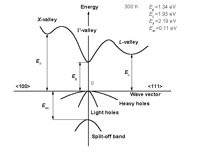
| Band gap | 1.344 eV (300 K; direct) |
| Electron mobility | 5400 cm2/(V·s) (300 K) |
| Thermal conductivity | 0.68 W/(cm·K) (300 K) |
Refractive index (nD) | 3.1 (infrared); 3.55 (632.8 nm) [2] |
| Structure | |
| Zinc blende | |
| Tetrahedral | |
| Thermochemistry [4] | |
Heat capacity (C) | 45.4 J/(mol·K) |
Std molar entropy (S⦵298) | 59.8 J/(mol·K) |
Std enthalpy of formation (ΔfH⦵298) | −88.7 kJ/mol |
Gibbs free energy (ΔfG⦵) | −77.0 kJ/mol |
| Hazards | |
| Occupational safety and health (OHS/OSH): | |
Main hazards | Toxic, hydrolysis to phosphine |
| Safety data sheet (SDS) | External MSDS |
| Related compounds | |
Other anions | Indium nitride Indium arsenide Indium antimonide |
Other cations | Aluminium phosphide Gallium phosphide |
Related compounds | Indium gallium phosphide Aluminium gallium indium phosphide Gallium indium arsenide antimonide phosphide |
Except where otherwise noted, data are given for materials in their standard state (at 25 °C [77 °F], 100 kPa). | |
Indium phosphide (InP) is a binary semiconductor composed of indium and phosphorus. It has a face-centered cubic ("zincblende") crystal structure, identical to that of GaAs and most of the III-V semiconductors.
