Related Research Articles

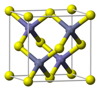
Gallium arsenide (GaAs) is a III-V direct band gap semiconductor with a zinc blende crystal structure.
A heterojunction bipolar transistor (HBT) is a type of bipolar junction transistor (BJT) that uses different semiconductor materials for the emitter and base regions, creating a heterojunction. The HBT improves on the BJT in that it can handle signals of very high frequencies, up to several hundred GHz. It is commonly used in modern ultrafast circuits, mostly radio frequency (RF) systems, and in applications requiring a high power efficiency, such as RF power amplifiers in cellular phones. The idea of employing a heterojunction is as old as the conventional BJT, dating back to a patent from 1951. Detailed theory of heterojunction bipolar transistor was developed by Herbert Kroemer in 1957.
Indium gallium phosphide (InGaP), also called gallium indium phosphide (GaInP), is a semiconductor composed of indium, gallium and phosphorus. It is used in high-power and high-frequency electronics because of its superior electron velocity with respect to the more common semiconductors silicon and gallium arsenide.
Thermophotovoltaic (TPV) energy conversion is a direct conversion process from heat to electricity via photons. A basic thermophotovoltaic system consists of a hot object emitting thermal radiation and a photovoltaic cell similar to a solar cell but tuned to the spectrum being emitted from the hot object.
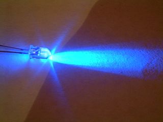
Indium gallium nitride is a semiconductor material made of a mix of gallium nitride (GaN) and indium nitride (InN). It is a ternary group III/group V direct bandgap semiconductor. Its bandgap can be tuned by varying the amount of indium in the alloy. InxGa1−xN has a direct bandgap span from the infrared for InN to the ultraviolet of GaN. The ratio of In/Ga is usually between 0.02/0.98 and 0.3/0.7.
Indium arsenide, InAs, or indium monoarsenide, is a narrow-bandgap semiconductor composed of indium and arsenic. It has the appearance of grey cubic crystals with a melting point of 942 °C.
Aluminium gallium indium phosphide is a semiconductor material that provides a platform for the development of multi-junction photovoltaics and optoelectronic devices. It has a direct bandgap ranging from ultraviolet to infrared photon energies.
Gallium arsenide phosphide is a semiconductor material, an alloy of gallium arsenide and gallium phosphide. It exists in various composition ratios indicated in its formula by the fraction x.

Aluminium antimonide (AlSb) is a semiconductor of the group III-V family containing aluminium and antimony. The lattice constant is 0.61 nm. The indirect bandgap is approximately 1.6 eV at 300 K, whereas the direct band gap is 2.22 eV.
Gallium antimonide (GaSb) is a semiconducting compound of gallium and antimony of the III-V family. It has a room temperature lattice constant of about 0.610 nm. It has a room temperature direct bandgap of approximately 0.73 eV.

Multi-junction (MJ) solar cells are solar cells with multiple p–n junctions made of different semiconductor materials. Each material's p–n junction will produce electric current in response to different wavelengths of light. The use of multiple semiconducting materials allows the absorbance of a broader range of wavelengths, improving the cell's sunlight to electrical energy conversion efficiency.
Indium arsenide antimonide phosphide is a semiconductor material.
Indium gallium arsenide phosphide is a quaternary compound semiconductor material, an alloy of gallium arsenide, gallium phosphide, indium arsenide, or indium phosphide. This compound has applications in photonic devices, due to the ability to tailor its band gap via changes in the alloy mole ratios, x and y.

Rubin Braunstein (1922–2018) was an American physicist and educator. In 1955 he published the first measurements of light emission by semiconductor diodes made from crystals of gallium arsenide (GaAs), gallium antimonide (GaSb), and indium phosphide (InP). GaAs, GaSb, and InP are examples of III-V semiconductors. The III-V semiconductors absorb and emit light much more strongly than silicon, which is the best-known semiconductor. Braunstein's devices are the forerunners of contemporary LED lighting and semiconductor lasers, which typically employ III-V semiconductors. The 2000 and 2014 Nobel Prizes in Physics were awarded for further advances in closely related fields.
Aluminium indium antimonide, also known as indium aluminium antimonide or AlInSb (AlxIn1-xSb), is a ternary III-V semiconductor compound. It can be considered as an alloy between aluminium antimonide and indium antimonide. The alloy can contain any ratio between aluminium and indium. AlInSb refers generally to any composition of the alloy.
Aluminium gallium antimonide, also known as gallium aluminium antimonide or AlGaSb (AlxGa1-xSb), is a ternary III-V semiconductor compound. It can be considered as an alloy between aluminium antimonide and gallium antimonide. The alloy can contain any ratio between aluminium and gallium. AlGaSb refers generally to any composition of the alloy.
Gallium arsenide antimonide, also known as gallium antimonide arsenide or GaAsSb, is a ternary III-V semiconductor compound; x indicates the fractions of arsenic and antimony in the alloy. GaAsSb refers generally to any composition of the alloy. It is an alloy of gallium arsenide (GaAs) and gallium antimonide (GaSb).
Indium arsenide antimonide, also known as indium antimonide arsenide or InAsSb (InAs1-xSbx), is a ternary III-V semiconductor compound. It can be considered as an alloy between indium arsenide (InAs) and indium antimonide (InSb). The alloy can contain any ratio between arsenic and antimony. InAsSb refers generally to any composition of the alloy.
Gallium indium antimonide, also known as indium gallium antimonide, GaInSb, or InGaSb (GaxIn1-xSb), is a ternary III-V semiconductor compound. It can be considered as an alloy between gallium antimonide and indium antimonide. The alloy can contain any ratio between gallium and indium. GaInSb refers generally to any composition of the alloy.
Aluminium arsenide antimonide, or AlAsSb (AlAs1-xSbx), is a ternary III-V semiconductor compound. It can be considered as an alloy between aluminium arsenide and aluminium antimonide. The alloy can contain any ratio between arsenic and antimony. AlAsSb refers generally to any composition of the alloy.
References
- ↑ Room temperature midinfrared electroluminescence from GaInAsSbP light emitting diodes, A. Krier, V. M. Smirnov, P. J. Batty, V. I. Vasil’ev, G. S. Gagis, and V. I. Kuchinskii, Appl. Phys. Lett. vol. 90 pp. 211115 (2007) doi : 10.1063/1.2741147
- 1 2 Lattice-matched GaInPAsSb/InAs structures for devices of infrared optoelectronics, M. Aidaraliev, N. V. Zotova, S. A. Karandashev, B. A. Matveev, M. A. Remennyi, N. M. Stus’, G. N. Talalakin, V. V. Shustov, V. V. Kuznetsov and E. A. Kognovitskaya, Semiconductors vol. 36 num. 8 pp. 944-949 (2002) doi : 10.1134/1.1500478
- ↑ Low Bandgap GaInAsSbP Pentanary Thermophotovoltaic Diodes, K. J. Cheetham, P. J. Carrington, N. B. Cook and A. Krier, Solar Energy Materials and Solar Cells, vol. 95 pp. 534-537 (2011) doi : 10.1016/j.solmat.2010.08.036
| | This condensed matter physics-related article is a stub. You can help Wikipedia by expanding it. |