Indium(III) sulfide

Last updated
Indium(III) sulfide
Names
Other names
Indium sesquisulfide
Diindium trisulfide
Identifiers
3D model (JSmol)
ChemSpider
ECHA InfoCard 100.031.571 OOjs UI icon edit-ltr-progressive.svg
PubChem CID
UNII
  • InChI=1S/2In.3S Yes check.svgY
    Key: ZOMNDSJRWSNDFL-UHFFFAOYSA-N Yes check.svgY
  • InChI=1/2In.3S/rIn2S3/c3-1-5-2-4
    Key: ZOMNDSJRWSNDFL-YYMIQOPKAJ
  • S=[In]S[In]=S
Properties
In2S3
Molar mass 325.82 g·mol−1
Appearancered powder
Density 4.90 g cm3, solid
Melting point 1,050 °C (1,920 °F; 1,320 K)
insoluble
Hazards
GHS labelling: [1]
GHS-pictogram-exclam.svg
Warning
H302+H332, H315, H319, H335
P280, P301+P330+P331, P302+P352, P304+P340, P312, P332+P313, P337+P313
NFPA 704 (fire diamond)
3
4
2
Except where otherwise noted, data are given for materials in their standard state (at 25 °C [77 °F], 100 kPa).
X mark.svgN  verify  (what is  Yes check.svgYX mark.svgN ?)

Indium(III) sulfide (Indium sesquisulfide, Indium sulfide (2:3), Indium (3+) sulfide) is the inorganic compound with the formula In 2 S 3.

Contents

It has a "rotten egg" odor characteristic of sulfur compounds, and produces hydrogen sulfide gas when reacted with mineral acids. [2]

Three different structures ("polymorphs") are known: yellow, α-In2S3 has a defect cubic structure, red β-In2S3 has a defect spinel, tetragonal, structure, and γ-In2S3 has a layered structure. The red, β, form is considered to be the most stable form at room temperature, although the yellow form may be present depending on the method of production. In2S3 is attacked by acids and by sulfide. It is slightly soluble in Na2S. [3]

Indium sulfide was the first indium compound ever described, being reported in 1863. [4] Reich and Richter determined the existence of indium as a new element from the sulfide precipitate.

Structure and properties

In2S3 features tetrahedral In(III) centers linked to four sulfido ligands.

α-In2S3 has a defect cubic structure. The polymorph undergoes a phase transition at 420 °C and converts to the spinel structure of β-In2S3. Another phase transition at 740 °C produces the layered γ-In2S3 polymorph. [5]

β-In2S3 has a defect spinel structure. The sulfide anions are closely packed in layers, with octahedrally-coordinated In(III) cations present within the layers, and tetrahedrally-coordinated In(III) cations between them. A portion of the tetrahedral interstices are vacant, which leads to the defects in the spinel. [6]

β-In2S3 has two subtypes. In the T-In2S3 subtype, the tetragonally-coordinated vacancies are in an ordered arrangement, whereas the vacancies in C-In2S3 are disordered. The disordered subtype of β-In2S3 shows activity for photocatalytic H2 production with a noble metal cocatalyst, but the ordered subtype does not. [7]

β-In2S3 is an N-type semiconductor with an optical band gap of 2.1 eV. It has been proposed to replace the hazardous cadmium sulfide, CdS, as a buffer layer in solar cells, [8] and as an additional semiconductor to increase the performance of TiO2-based photovoltaics. [7]

The unstable γ-In2S3 polymorph has a layered structure.

Production

Indium sulfide is usually prepared by direct combination of the elements.

Production from volatile complexes of indium and sulfur, for example dithiocarbamates (e.g. Et2InIIIS2CNEt2), has been explored for vapor deposition techniques. [9]

Thin films of the beta complex can be grown by chemical spray pyrolysis. Solutions of In(III) salts and organic sulfur compounds (often thiourea) are sprayed onto preheated glass plates, where the chemicals react to form thin films of indium sulfide. [10] Changing the temperature at which the chemicals are deposited and the In:S ratio can affect the optical band gap of the film. [11]

Single-walled indium sulfide nanotubes can be formed in the laboratory, by the use of two solvents (one in which the compound dissolves poorly and one in which it dissolves well). There is partial replacement of the sulfido ligands with O2, and the compound forms thin nanocoils, which self-assemble into arrays of nanotubes with diameters on the order of 10 nm, and walls approximately 0.6 nm thick. The process mimics protein crystallization. [12]

Indium(III) sulfide nanocoils (a), nanotubes (b), and their ordered arrays (d-f). Scale bars: a,d,e,f - 50 nm; b - 100 nm. Indium(III) sulfide nanotubes.jpg
Indium(III) sulfide nanocoils (a), nanotubes (b), and their ordered arrays (d-f). Scale bars: a,d,e,f - 50 nm; b - 100 nm.

Safety

The β-In2S3 polymorph, in powdered form, can irritate eyes, skin and respiratory organs. It is toxic if swallowed, but can be handled safely under conventional laboratory conditions. It should be handled with gloves, and care should be taken to keep from inhaling the compound, and to keep it from contact with the eyes. [13]

Applications

Photovoltaic and Photocatalytic

There is considerable interest in using In2S3 to replace the semiconductor CdS (cadmium sulfide) in photoelectronic devices. β-In2S3 has a tunable band gap, which makes it attractive for photovoltaic applications, [11] and it shows promise when used in conjunction with TiO2 in solar panels, indicating that it could replace CdS in that application as well. [7] Cadmium sulfide is toxic and must be deposited with a chemical bath, [14] but indium(III) sulfide shows few adverse biological effects and can be deposited as a thin film through less hazardous methods. [11] [14]

Thin films β-In2S3 can be grown with varying band gaps, which make them widely applicable as photovoltaic semiconductors, especially in heterojunction solar cells. [11]

Plates coated with beta-In2S3 nanoparticles can be used efficiently for PEC (photoelectrochemical) water splitting. [15]

Biomedical

A preparation of indium sulfide made with the radioactive 113In can be used as a lung scanning agent for medical imaging. [16] It is taken up well by lung tissues, but does not accumulate there.

Other

In2S3 nanoparticles luminesce in the visible spectrum. Preparing In2S3 nanoparticles in the presence of other heavy metal ions creates highly efficient blue, green, and red phosphors, which can be used in projectors and instrument displays. [17]

Related Research Articles

<span class="mw-page-title-main">Organic electronics</span> Field of materials science

Organic electronics is a field of materials science concerning the design, synthesis, characterization, and application of organic molecules or polymers that show desirable electronic properties such as conductivity. Unlike conventional inorganic conductors and semiconductors, organic electronic materials are constructed from organic (carbon-based) molecules or polymers using synthetic strategies developed in the context of organic chemistry and polymer chemistry.

Indium tin oxide (ITO) is a ternary composition of indium, tin and oxygen in varying proportions. Depending on the oxygen content, it can be described as either a ceramic or an alloy. Indium tin oxide is typically encountered as an oxygen-saturated composition with a formulation of 74% In, 18% Sn, and 8% O by weight. Oxygen-saturated compositions are so typical that unsaturated compositions are termed oxygen-deficient ITO. It is transparent and colorless in thin layers, while in bulk form it is yellowish to gray. In the infrared region of the spectrum it acts as a metal-like mirror.

<span class="mw-page-title-main">Cadmium sulfide</span> Chemical compound

Cadmium sulfide is the inorganic compound with the formula CdS. Cadmium sulfide is a yellow solid. It occurs in nature with two different crystal structures as the rare minerals greenockite and hawleyite, but is more prevalent as an impurity substituent in the similarly structured zinc ores sphalerite and wurtzite, which are the major economic sources of cadmium. As a compound that is easy to isolate and purify, it is the principal source of cadmium for all commercial applications. Its vivid yellow color led to its adoption as a pigment for the yellow paint "cadmium yellow" in the 18th century.

<span class="mw-page-title-main">Cadmium selenide</span> Chemical compound

Cadmium selenide is an inorganic compound with the formula CdSe. It is a black to red-black solid that is classified as a II-VI semiconductor of the n-type. It is a pigment but applications are declining because of environmental concerns

<span class="mw-page-title-main">Indium gallium nitride</span> Chemical compound

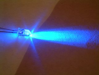
Indium gallium nitride is a semiconductor material made of a mix of gallium nitride (GaN) and indium nitride (InN). It is a ternary group III/group V direct bandgap semiconductor. Its bandgap can be tuned by varying the amount of indium in the alloy. InxGa1−xN has a direct bandgap span from the infrared for InN to the ultraviolet of GaN. The ratio of In/Ga is usually between 0.02/0.98 and 0.3/0.7.

Hybrid solar cells combine advantages of both organic and inorganic semiconductors. Hybrid photovoltaics have organic materials that consist of conjugated polymers that absorb light as the donor and transport holes. Inorganic materials in hybrid cells are used as the acceptor and electron transporter in the structure. The hybrid photovoltaic devices have a potential for not only low-cost by roll-to-roll processing but also for scalable solar power conversion.

<span class="mw-page-title-main">Gallium(III) oxide</span> Chemical compound

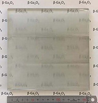
Gallium(III) oxide is an inorganic compound and ultra-wide bandgap semiconductor with the formula Ga2O3. It is actively studied for applications in power electronics, phosphors, and gas sensing. The compound has several polymorphs, of which the monoclinic β-phase is the most stable. The β-phase’s bandgap of 4.7–4.9 eV and large-area, native substrates make it a promising competitor to GaN and SiC-based power electronics applications and solar-blind UV photodetectors. Ga2O3 exhibits reduced thermal conductivity and electron mobility by an order of magnitude compared to GaN and SiC, but is predicted to be significantly more cost-effective due to being the only wide-bandgap material capable of being grown from melt. β-Ga2O3 is thought to be radiation hard which makes it promising for military and space applications.

<span class="mw-page-title-main">Bismuth subcarbonate</span> Chemical compound

Bismuth subcarbonate (BiO)2CO3, sometimes written Bi2O2(CO3) is a chemical compound of bismuth containing both oxide and carbonate anions. Bismuth is in the +3 oxidation state. Bismuth subcarbonate occurs naturally as the mineral bismutite. Its structure consists of Bi–O layers and CO3 layers and is related to kettnerite, CaBi(CO3)OF. It is light-sensitive.

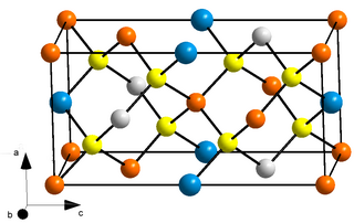
Indium(III) selenide is a compound of indium and selenium. It has potential for use in photovoltaic devices and it has been the subject of extensive research. The two most common phases, α and β, have a layered structure, while γ is a "defect wurtzite structure." In all, five polymorpsare known: α, β, γ, δ, κ. The α- β phase transition is accompanied by a change in electrical conductivity. The band-gap of γ-In2Se3 is approximately 1.9 eV.

The indium chalcogenides include all compounds of indium with the chalcogen elements, oxygen, sulfur, selenium and tellurium. (Polonium is excluded as little is known about its compounds with indium). The best-characterised compounds are the In(III) and In(II) chalcogenides e.g. the sulfides In2S3 and InS.
This group of compounds has attracted a lot of research attention because they include semiconductors, photovoltaics and phase-change materials. In many applications indium chalcogenides are used as the basis of ternary and quaternary compounds such as indium tin oxide, ITO and copper indium gallium selenide, CIGS.

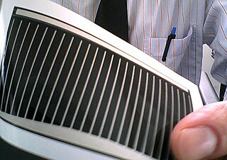
Organic photovoltaic devices (OPVs) are fabricated from thin films of organic semiconductors, such as polymers and small-molecule compounds, and are typically on the order of 100 nm thick. Because polymer based OPVs can be made using a coating process such as spin coating or inkjet printing, they are an attractive option for inexpensively covering large areas as well as flexible plastic surfaces. A promising low cost alternative to conventional solar cells made of crystalline silicon, there is a large amount of research being dedicated throughout industry and academia towards developing OPVs and increasing their power conversion efficiency.

Tin(II) sulfide is a chemical compound of tin and sulfur. The chemical formula is SnS. Its natural occurrence concerns herzenbergite (α-SnS), a rare mineral. At elevated temperatures above 905 K, SnS undergoes a second order phase transition to β-SnS (space group: Cmcm, No. 63). In recent years, it has become evident that a new polymorph of SnS exists based upon the cubic crystal system, known as π-SnS (space group: P213, No. 198).

<span class="mw-page-title-main">Copper indium gallium selenide solar cell</span>

A copper indium gallium selenide solar cell is a thin-film solar cell used to convert sunlight into electric power. It is manufactured by depositing a thin layer of copper indium gallium selenide solution on glass or plastic backing, along with electrodes on the front and back to collect current. Because the material has a high absorption coefficient and strongly absorbs sunlight, a much thinner film is required than of other semiconductor materials.

<span class="mw-page-title-main">Transparent conducting film</span> Optically transparent and electrically conductive material

Transparent conducting films (TCFs) are thin films of optically transparent and electrically conductive material. They are an important component in a number of electronic devices including liquid-crystal displays, OLEDs, touchscreens and photovoltaics. While indium tin oxide (ITO) is the most widely used, alternatives include wider-spectrum transparent conductive oxides (TCOs), conductive polymers, metal grids and random metallic networks, carbon nanotubes (CNT), graphene, nanowire meshes and ultra thin metal films.

<span class="mw-page-title-main">CZTS</span> Chemical compound

Copper zinc tin sulfide (CZTS) is a quaternary semiconducting compound which has received increasing interest since the late 2000s for applications in thin film solar cells. The class of related materials includes other I2-II-IV-VI4 such as copper zinc tin selenide (CZTSe) and the sulfur-selenium alloy CZTSSe. CZTS offers favorable optical and electronic properties similar to CIGS (copper indium gallium selenide), making it well suited for use as a thin-film solar cell absorber layer, but unlike CIGS (or other thin films such as CdTe), CZTS is composed of only abundant and non-toxic elements. Concerns with the price and availability of indium in CIGS and tellurium in CdTe, as well as toxicity of cadmium have been a large motivator to search for alternative thin film solar cell materials. The power conversion efficiency of CZTS is still considerably lower than CIGS and CdTe, with laboratory cell records of 11.0 % for CZTS and 12.6 % for CZTSSe as of 2019.

<span class="mw-page-title-main">Indium acetylacetonate</span> Chemical compound

Indium acetylacetonate, also known as In(acac)3, is a compound with formula In(C5H7O2)3. It is a colorless solid. It adopts an octahedral structure.

<span class="mw-page-title-main">Gallium(III) sulfide</span> Chemical compound

Gallium(III) sulfide, Ga2S3, is a compound of sulfur and gallium, that is a semiconductor that has applications in electronics and photonics.

Indium(II) selenide (InSe) is an inorganic compound composed of indium and selenium. It is a III-VI layered semiconductor. The solid has a structure consisting of two-dimensional layers bonded together only by van der Waals forces. Each layer has the atoms in the order Se-In-In-Se.

<span class="mw-page-title-main">Cerium(III) sulfide</span> Chemical compound

Cerium(III) sulfide, also known as cerium sesquisulfide, is an inorganic compound with the formula Ce2S3. It is the sulfide salt of cerium(III) and exists as three polymorphs with different crystal structures.

References

  1. GHS: Alpha Aesar 045563
  2. Indium Sulfide. indium.com
  3. Indium Sulfide. indium.com
  4. Reich, F.; Richter, Th. (1863). "Vorläufige Notiz über ein neues Metal". J. Prakt. Chem. (in German). 89: 441–448. doi:10.1002/prac.18630890156.
  5. Bahadur, D. Inorganic Materials: Recent Advances. Alpha Sciences International, Ltd., 2004. 106
  6. Steigmann, G.A.; Sutherland, H.H.; Goodyear, J. (1965). “The Crystal Structure of -In2S3 “. Acta Crystallogr. , 19: 967-971.
  7. 1 2 3 Chai, B.; Peng, T.; Zeng, P.; Mao, J. (2011.) “Synthesis of Floriated In2S3 Decorated With TiO2 Nanoparticles for Photocatalytic Hydrogen Production Under Visible Light.” J. Mater. Chem. , 21: 14587. doi : 10.1039/c1jm11566a.
  8. Barreau, N.; Marsillac, S.; Albertini, D.; Bernede, J.C. (2002). "Structural, optical and electrical properties of β-In2S3-3xO3x thin films obtained by PVD". Thin Solid Films . 403: 331–334.
  9. Haggata, S. W.; Malik, M. Azad; Motevalli, M.; O'Brien, P.; Knowles, J. C. (1995). "Synthesis and Characterization of Some Mixed Alkyl Thiocarbamates of Gallium and Indium, Precursors for III/VI Materials: The X-ray Single-Crystal Structures of Dimethyl- and Diethylindium Diethyldithiocarbamate". Chem. Mater. 7 (4): 716–724. doi : 10.1021/cm00052a017.
  10. Otto, K.; Katarski, A.; Mere, O.; Volobujeva, M. (2009). “Spray Pyrolysis Deposition of Indium Sulphide Thin Films.” Thin Solid Films , 519(10): 3055-3060. doi : 10.1016/j.tsf.2010.12.027
  11. 1 2 3 4 Calixto-Rodriguez, M.; Tiburcio-Silver, A.; Ortiz, A.; Sanchez-Juarez, A. (2004.) “Optoelectronical Properties of Indium Sulfide Thin Films Prepared by Spray Pyrolysis for Photovoltaic Applications.” Thin Solid Films , 480: 133-137. doi : 10.1016/j/tsf.2004.11.046.
  12. 1 2 Ni, Bing; Liu, Huiling; Wang, Peng-Peng; He, Jie; Wang, Xun (2015). "General synthesis of inorganic single-walled nanotubes". Nat. Commun. 6: 8756. Bibcode:2015NatCo...6.8756N. doi: 10.1038/ncomms9756 . PMC   4640082 . PMID   26510862.
  13. Sigma-Aldrich. (2015) “Safety Data Sheet Version 4.5.” Aldrich – 308293.
  14. 1 2 Karthikeyan, S.; Hill, A.E.; Pilkington, R.D. (2016). “Low Temperature Pulsed Direct Current Magnetron Sputtering Technique for Single Phase -In2S3 Buffer Layers for Solar Cell Applications.” Appl. Surf. Sci. 418: 199-206. doi : 10.1016/j.apsusc.2017.01.14
  15. Tian, Y.; Wang, L.; Tang, H.; Zhou, W. (2015). “Ultrathin Two-Dimensional -In2S3 Nanocrystals: Oriented-AttachmentGrowth Controlled By Metal Ions and Photoelectrochemical Properties.” J. Mater. Chem. A , 3: 11294, doi : 10.1039/c5ta01958c.
  16. Csetenyi, J.; Szamel, S.I.; Fyzy, M.; Karika, Z. (1974). “Albumin Macroaggregates Containing 113mIn-sulfide (113mIn SMAA): Technique for the Preparation of a New Lung Scanning Agent.” Proc. Int. Symp. Nucl. Med. , 3: 293-301.
  17. Chen, W.; Bovin, J.; Joly, A.; Wang, S.; Su, F.; Li, G. (2004). “Full-Color Emission from In2S3 and In2S3:Eu3+ Nanoparticles.” J. Phys. Chem. B , 108: 11927-11934. doi : 10.1021/jp048107m.

General references