Indium gallium nitride

Last updated

InGaN blue LED (380-405 nm) Uv-LED.jpg
InGaN blue LED (380–405 nm)
Spectrum of a white-light LED where GaN or InGaN blue source pumps Ce:YAG phosphor White LED.png
Spectrum of a white-light LED where GaN or InGaN blue source pumps Ce:YAG phosphor

Indium gallium nitride (InGaN, In x Ga 1−x N ) is a semiconductor material made of a mix of gallium nitride (GaN) and indium nitride (InN). It is a ternary group III/group V direct bandgap semiconductor. Its bandgap can be tuned by varying the amount of indium in the alloy. InxGa1−xN has a direct bandgap span from the infrared (0.69 eV) for InN to the ultraviolet (3.4 eV) of GaN. The ratio of In/Ga is usually[ clarification needed ] between 0.02/0.98 and 0.3/0.7. [1]

Contents

Applications

LEDs

Indium gallium nitride is the light-emitting layer in modern blue and green LEDs and often grown on a GaN buffer on a transparent substrate as, e.g. sapphire or silicon carbide. It has a high heat capacity and its sensitivity to ionizing radiation is low (like other group III nitrides), making it also a potentially suitable material for solar photovoltaic devices, specifically for arrays for satellites.

It is theoretically predicted that spinodal decomposition of indium nitride should occur for compositions between 15% and 85%, leading to In-rich and Ga-rich InGaN regions or clusters. However, only a weak phase segregation has been observed in experimental local structure studies. [2] Other experimental results using cathodoluminescence and photoluminescence excitation on low In-content InGaN multi-quantum wells have demonstrated that providing correct material parameters of the InGaN/GaN alloys, theoretical approaches for AlGaN/GaN systems also apply to InGaN nanostructures. [3]

GaN is a defect-rich material with typical dislocation densities [4] exceeding 108 cm−2. Light emission from InGaN layers grown on such GaN buffers used in blue and green LEDs is expected to be attenuated because of non-radiative recombination at such defects. [5] Nevertheless, InGaN quantum wells, are efficient light emitters in green, blue, white and ultraviolet light-emitting diodes and diode lasers. [6] [7] [8] The indium-rich regions have a lower bandgap than the surrounding material and create regions of reduced potential energy for charge carriers. Electron-hole pairs are trapped there and recombine with emission of light, instead of diffusing to crystal defects where the recombination is non-radiative. Also, self-consistent computer simulations have shown that radiative recombination is focused where regions are rich of indium. [9]

The emitted wavelength, dependent on the material's band gap, can be controlled by the GaN/InN ratio, from near ultraviolet for 0.02In/0.98Ga through 390 nm for 0.1In/0.9Ga, violet-blue 420 nm for 0.2In/0.8Ga, to blue 440 nm for 0.3In/0.7Ga, to red for higher ratios and also by the thickness of the InGaN layers which are typically in the range of 2–3 nm [ citation needed ]. However, atomistic simulations results have shown that emission energies have a minor dependence on small variations of device dimensions. [10] Studies based on device simulation have shown that it could be possible to increase InGaN/GaN LED efficiency using band gap engineering, especially for green LEDs. [11]

Photovoltaics

The ability to perform bandgap engineering with InGaN over a range that provides a good spectral match to sunlight, makes InGaN suitable for solar photovoltaic cells. [12] [13] It is possible to grow multiple layers with different bandgaps, as the material is relatively insensitive to defects introduced by a lattice mismatch between the layers. A two-layer multijunction cell with bandgaps of 1.1 eV and 1.7 eV can attain a theoretical 50% maximum efficiency, and by depositing multiple layers tuned to a wide range of bandgaps an efficiency up to 70% is theoretically expected. [14]

Significant photoresponse was obtained from experimental InGaN single-junction devices. [15] [16] In addition to controlling the optical properties, [17] which results in band gap engineering, photovoltaic device performance can be improved by engineering the microstructure of the material to increase the optical path length and provide light trapping. Growing nanocolumns on the device can further result in resonant interaction with light, [18] and InGaN nanocolumns have been successfully deposited on SiO
2
using plasma enhanced evaporation. [19] Nanorod growth may also be advantageous in the reduction of treading dislocations which may act as charge traps reducing solar cell efficiency [20]

Metal-modulated epitaxy allows controlled atomic layer-by-layer growth of thin films with almost ideal characteristics enabled by strain relaxation at the first atomic layer. The crystal's lattice structures match up, resembling a perfect crystal, with corresponding luminosity. The crystal had indium content ranging from x ~ 0.22 to 0.67. Significant improvement in the crystalline quality and optical properties began at x ~ 0.6. Films were grown at ~400 °C to facilitate indium incorporation and with precursor modulation to enhance surface morphology and metal adlayer diffusion. These findings should contribute to the development of growth techniques for nitride semiconductors under high lattice misfit conditions. [21] [22]

Quantum heterostructures

Quantum heterostructures are often built from GaN with InGaN active layers. InGaN can be combined with other materials, e.g. GaN, AlGaN, on SiC, sapphire and even silicon.

Nanorods

InGaN nanorod LEDs are three-dimensional structures with a larger emitting surface, better efficiency and greater light emission compared to planar LEDs [ citation needed ].

Safety and toxicity

The toxicology of InGaN has not been fully investigated. The dust is an irritant to skin, eyes and lungs. The environment, health and safety aspects of indium gallium nitride sources (such as trimethylindium, trimethylgallium and ammonia) and industrial hygiene monitoring studies of standard MOVPE sources have been reported recently in a review. [23]

See also

Related Research Articles

<span class="mw-page-title-main">Band gap</span> Energy range in a solid where no electron states exist

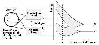
In solid-state physics and solid-state chemistry, a band gap, also called a bandgap or energy gap, is an energy range in a solid where no electronic states exist. In graphs of the electronic band structure of solids, the band gap refers to the energy difference between the top of the valence band and the bottom of the conduction band in insulators and semiconductors. It is the energy required to promote an electron from the valence band to the conduction band. The resulting conduction-band electron are free to move within the crystal lattice and serve as charge carriers to conduct electric current. It is closely related to the HOMO/LUMO gap in chemistry. If the valence band is completely full and the conduction band is completely empty, then electrons cannot move within the solid because there are no available states. If the electrons are not free to move within the crystal lattice, then there is no generated current due to no net charge carrier mobility. However, if some electrons transfer from the valence band to the conduction band, then current can flow. Therefore, the band gap is a major factor determining the electrical conductivity of a solid. Substances having large band gaps are generally insulators, those with small band gaps are semiconductor, and conductors either have very small band gaps or none, because the valence and conduction bands overlap to form a continuous band.

<span class="mw-page-title-main">Laser diode</span> Semiconductor laser

A laser diode is a semiconductor device similar to a light-emitting diode in which a diode pumped directly with electrical current can create lasing conditions at the diode's junction.

<span class="mw-page-title-main">Gallium arsenide</span> Chemical compound

Gallium arsenide (GaAs) is a III-V direct band gap semiconductor with a zinc blende crystal structure.

Wide-bandgap semiconductors are semiconductor materials which have a larger band gap than conventional semiconductors. Conventional semiconductors like silicon have a bandgap in the range of 0.6 – 1.5 electronvolt (eV), whereas wide-bandgap materials have bandgaps in the range above 2 eV. Generally, wide-bandgap semiconductors have electronic properties which fall in between those of conventional semiconductors and insulators.

<span class="mw-page-title-main">Gallium nitride</span> Chemical compound

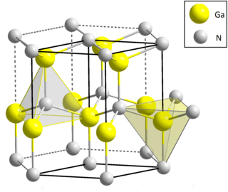
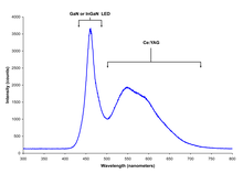
Gallium nitride is a binary III/V direct bandgap semiconductor commonly used in blue light-emitting diodes since the 1990s. The compound is a very hard material that has a Wurtzite crystal structure. Its wide band gap of 3.4 eV affords it special properties for applications in optoelectronic, high-power and high-frequency devices. For example, GaN is the substrate which makes violet (405 nm) laser diodes possible, without requiring nonlinear optical frequency-doubling.

<span class="mw-page-title-main">Quantum well</span> Concept in quantum mechanics

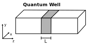
A quantum well is a potential well with only discrete energy values.

<span class="mw-page-title-main">Indium nitride</span> Chemical compound

Indium nitride is a small bandgap semiconductor material which has potential application in solar cells and high speed electronics.

Indium gallium phosphide (InGaP), also called gallium indium phosphide (GaInP), is a semiconductor composed of indium, gallium and phosphorus. It is used in high-power and high-frequency electronics because of its superior electron velocity with respect to the more common semiconductors silicon and gallium arsenide.

Indium gallium arsenide (InGaAs) is a ternary alloy of indium arsenide (InAs) and gallium arsenide (GaAs). Indium and gallium are group III elements of the periodic table while arsenic is a group V element. Alloys made of these chemical groups are referred to as "III-V" compounds. InGaAs has properties intermediate between those of GaAs and InAs. InGaAs is a room-temperature semiconductor with applications in electronics and photonics.

Thermophotovoltaic (TPV) energy conversion is a direct conversion process from heat to electricity via photons. A basic thermophotovoltaic system consists of a hot object emitting thermal radiation and a photovoltaic cell similar to a solar cell but tuned to the spectrum being admitted from the hot object.

Aluminium gallium indium phosphide is a semiconductor material that provides a platform for the development of novel multi-junction photovoltaics and optoelectronic devices, as it spans a direct bandgap from deep ultraviolet to infrared.

<span class="mw-page-title-main">Quantum dot solar cell</span> Type of solar cell based on quantum dot devices

A quantum dot solar cell (QDSC) is a solar cell design that uses quantum dots as the captivating photovoltaic material. It attempts to replace bulk materials such as silicon, copper indium gallium selenide (CIGS) or cadmium telluride (CdTe). Quantum dots have bandgaps that are adjustable across a wide range of energy levels by changing their size. In bulk materials, the bandgap is fixed by the choice of material(s). This property makes quantum dots attractive for multi-junction solar cells, where a variety of materials are used to improve efficiency by harvesting multiple portions of the solar spectrum.

Third-generation photovoltaic cells are solar cells that are potentially able to overcome the Shockley–Queisser limit of 31–41% power efficiency for single bandgap solar cells. This includes a range of alternatives to cells made of semiconducting p-n junctions and thin film cells. Common third-generation systems include multi-layer ("tandem") cells made of amorphous silicon or gallium arsenide, while more theoretical developments include frequency conversion,, hot-carrier effects and other multiple-carrier ejection techniques.

<span class="mw-page-title-main">Multi-junction solar cell</span> Solar power cell with multiple band gaps from different materials

Multi-junction (MJ) solar cells are solar cells with multiple p–n junctions made of different semiconductor materials. Each material's p-n junction will produce electric current in response to different wavelengths of light. The use of multiple semiconducting materials allows the absorbance of a broader range of wavelengths, improving the cell's sunlight to electrical energy conversion efficiency.

<span class="mw-page-title-main">Shockley–Queisser limit</span> Maximum theoretical efficiency of a solar cell

In physics, the radiative efficiency limit is the maximum theoretical efficiency of a solar cell using a single p-n junction to collect power from the cell where the only loss mechanism is radiative recombination in the solar cell. It was first calculated by William Shockley and Hans-Joachim Queisser at Shockley Semiconductor in 1961, giving a maximum efficiency of 30% at 1.1 eV. The limit is one of the most fundamental to solar energy production with photovoltaic cells, and is one of the field's most important contributions.
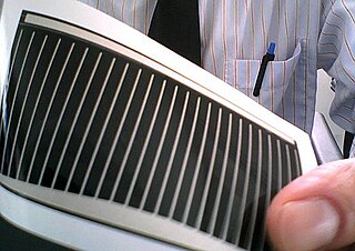
<span class="mw-page-title-main">Copper indium gallium selenide solar cell</span>

A copper indium gallium selenide solar cell is a thin-film solar cell used to convert sunlight into electric power. It is manufactured by depositing a thin layer of copper indium gallium selenide solid solution on glass or plastic backing, along with electrodes on the front and back to collect current. Because the material has a high absorption coefficient and strongly absorbs sunlight, a much thinner film is required than of other semiconductor materials.

Two-photon photovoltaic effect is an energy collection method based on two-photon absorption (TPA). The TPP effect can be thought of as the nonlinear equivalent of the traditional photovoltaic effect involving high optical intensities. This effect occurs when two photons are absorbed at the same time resulting in an electron-hole pair.

<span class="mw-page-title-main">Solar Frontier</span>

Solar Frontier Kabushiki Kaisha is a Japanese photovoltaic company that develops and manufactures thin film solar cells using CIGS technology. It is a fully owned subsidiary of Showa Shell Sekiyu and located in Minato, Tokyo, Japan. The company was founded in 2006 as Showa Shell Solar, and renamed Solar Frontier in April 2010.

Light-emitting diodes (LEDs) produce light by the recombination of electrons and electron holes in a semiconductor, a process called "electroluminescence". The wavelength of the light produced depends on the energy band gap of the semiconductors used. Since these materials have a high index of refraction, design features of the devices such as special optical coatings and die shape are required to efficiently emit light. A LED is a long-lived light source, but certain mechanisms can cause slow loss of efficiency of the device or sudden failure. The wavelength of the light emitted is a function of the band gap of the semiconductor material used; materials such as gallium arsenide, and others, with various trace doping elements, are used to produce different colors of light. Another type of LED uses a quantum dot which can have its properties and wavelength adjusted by its size. Light-emitting diodes are widely used in indicator and display functions, and white LEDs are displacing other technologies for general illumination purposes.

References

  1. Linti, G. "The Group 13 Metals Aluminium, Gallium, Indium and Thallium. Chemical Patterns and Peculiarities. Edited by Simon Aldridge and Anthony J. Downs.Angew. Chem". Angewandte Chemie International Edition. 50: 11569. doi:10.1002/anie.201105633.
  2. V. Kachkanov; K.P. O'Donnell; S. Pereira; R.W. Martin (2007). "Localization of excitation in InGaN epilayers" (PDF). Phil. Mag. 87 (13): 1999–2017. Bibcode:2007PMag...87.1999K. doi:10.1080/14786430701342164. S2CID   136950050.
  3. A. Reale1; A. Di Carlo; A. Vinattieri; M. Colocci; F. Rossi; N. Armani; C. Ferrari; G. Salviati; L. Lazzarini; V. Grillo (2005). "Investigation of the recombination dynamics in low In-content InGaN MQWs by means of cathodoluminescence and photoluminescence excitation". Physica Status Solidi C. 2 (2): 817–821. Bibcode:2005PSSCR...2..817R. doi:10.1002/pssc.200460305.{{cite journal}}: CS1 maint: numeric names: authors list (link)
  4. Rak Jun Choi; Hyung Jae Lee; Yoon-bong Hahn; Hyung Koun Cho (2004). "Structural and optical properties of InGaN/GaN triangular-shape quantum wells with different threading dislocation densities". Korean Journal of Chemical Engineering. 21: 292–295. doi:10.1007/BF02705411. S2CID   54212942.
  5. P. G. Eliseev. "Radiative processes in InGaN quantum wells". Archived from the original on 8 April 2013.
  6. Liang-Yi Chen; Ying-Yuan Huang; Chun-Hsiang Chang; Yu-Hsuan Sun; Yun-Wei Cheng; Min-Yung Ke; Cheng-Pin Chen; JianJang Huang (2010). "High performance InGaN/GaN nanorod light emitting diode arrays fabricated by nanosphere lithography and chemical mechanical polishing processes". Optics Express. 18 (8): 7664–7669. Bibcode:2010OExpr..18.7664C. doi: 10.1364/OE.18.007664 . PMID   20588606.
  7. HJ Chang; et alter. "Strong luminescence from strain relaxed InGaN/GaN nanotips for highly efficient light emitters" (PDF). Retrieved 20 September 2013.
  8. C Skierbiszewski1,2, P Perlin1,2, I Grzegory, Z R Wasilewski, M Siekacz, A Feduniewicz, P Wisniewski, J Borysiuk, P Prystawko, G Kamler, T Suski and S Porowski (2005). "High power blue–violet InGaN laser diodes grown on bulk GaN substrates by plasma-assisted molecular beam epitaxy". Semiconductor Science and Technology. 20 (8): 809–813. Bibcode:2005SeScT..20..809S. doi:10.1088/0268-1242/20/8/030. S2CID   97464128.{{cite journal}}: CS1 maint: multiple names: authors list (link) CS1 maint: numeric names: authors list (link)
  9. Sacconi, F.; Auf der Maur, M.; Pecchia, A.; Lopez, M.; Di Carlo, A. (2012). "Optoelectronic properties of nanocolumnar InGaN/GaN quantum disk LEDs". Physica Status Solidi C. 9 (5): 1315–1319. Bibcode:2012PSSCR...9.1315S. doi: 10.1002/pssc.201100205 .
  10. M. Lopez, F. Sacconi, M. Auf der Maur, A. Pecchia, A. Di Carlo. "Atomistic simulation of InGaN/GaN quantum disk LEDs" (2012). "Atomistic simulation of InGaN/GaN quantum disk LEDs". Optical and Quantum Electronics. 44 (3): 89–94. doi:10.1007/s11082-012-9554-3. S2CID   126339984.{{cite journal}}: CS1 maint: multiple names: authors list (link)
  11. M. Auf der Maur, K. Lorenz and A. Di Carlo. "Band gap engineering approaches to increase InGaN/GaN LED efficiency" (2012). "Band gap engineering approaches to increase InGaN/GaN LED efficiency". Physica Status Solidi C. 44 (3–5): 83–88. doi:10.1007/s11082-011-9536-x. S2CID   11753092.
  12. McLaughlin, D.V.P.; Pearce, J.M. (2013). "Progress in Indium Gallium Nitride Materials for Solar Photovoltaic Energy Conversion". Metallurgical and Materials Transactions A. 44 (4): 1947–1954. Bibcode:2013MMTA...44.1947M. doi:10.1007/s11661-013-1622-1. S2CID   13952749.
  13. Bhuiyan, A.; Sugita, K.; Hashimoto, A.; Yamamoto, A. (2012). "InGaN Solar Cells: Present State of the Art and Important Challenges". IEEE Journal of Photovoltaics. 2 (3): 276–293. doi:10.1109/JPHOTOV.2012.2193384. S2CID   22027530.
  14. A nearly perfect solar cell, part 2 Archived 17 September 2020 at the Wayback Machine . Lbl.gov. Retrieved on 2011-11-07.
  15. Zeng, S. W.; et al. (2009). "Substantial photo-response of InGaN p–i–n homojunction solar cells". Semicond. Sci. Technol. 24 (5): 055009. Bibcode:2009SeScT..24e5009Z. doi:10.1088/0268-1242/24/5/055009. S2CID   97236733.
  16. Sun, X.; et al. (2008). "Photoelectric characteristics of metal/InGaN/GaN heterojunction structure". J. Phys. D. 41 (16): 165108. Bibcode:2008JPhD...41p5108S. doi:10.1088/0022-3727/41/16/165108. S2CID   120480676.
  17. Dirk V. P. McLaughlin; J.M. Pearce (2012). "Analytical Model for the Optical Functions of Indium Gallium Nitride with Application to Thin Film Solar Photovoltaic Cells". Materials Science and Engineering: B. 177 (2): 239–244. arXiv: 1201.2911 . doi:10.1016/j.mseb.2011.12.008. S2CID   95949405.
  18. Cao, L.; White, J. S.; Park, J. S.; Schuller, J. A.; Clemens, B. M.; Brongersma, M. L. (2009). "Engineering light absorption in semiconductor nanowire devices". Nature Materials. 8 (8): 643–647. Bibcode:2009NatMa...8..643C. doi:10.1038/nmat2477. PMID   19578337.
  19. S. Keating; M.G. Urquhart; D.V.P. McLaughlin; J.M. Pearce (2011). "Effects of Substrate Temperature on Indium Gallium Nitride Nanocolumn Crystal Growth". Crystal Growth & Design. 11 (2): 565–568. arXiv: 1203.0645 . doi:10.1021/cg101450n. S2CID   53506014.
  20. Cherns, D.; Webster, R. F.; Novikov, S. V.; Foxon, C. T.; Fischer, A. M.; Ponce, F. A.; Haigh, S. J. (2014). "Compositional variations in In0.5Ga0.5N nanorods grown by molecular beam epitaxy". Nanotechnology. 25 (21): 215705. Bibcode:2014Nanot..25u5705C. doi: 10.1088/0957-4484/25/21/215705 . PMID   24785272.
  21. "Controlled atomic-layer crystal growth is 'breakthrough' for solar-cell efficiency". KurzweilAI. Retrieved 31 October 2013.
  22. Fischer, A. M.; Wei, Y. O.; Ponce, F. A.; Moseley, M.; Gunning, B.; Doolittle, W. A. (2013). "Highly luminescent, high-indium-content InGaN film with uniform composition and full misfit-strain relaxation". Applied Physics Letters. 103 (13): 131101. Bibcode:2013ApPhL.103m1101F. doi:10.1063/1.4822122.
  23. D V Shenai-Khatkhate; R Goyette; R L DiCarlo; G Dripps (2004). "Environment, health and safety issues for sources used in MOVPE growth of compound semiconductors". Journal of Crystal Growth. 1–4 (1–4): 816–821. Bibcode:2004JCrGr.272..816S. doi:10.1016/j.jcrysgro.2004.09.007.