This article needs additional citations for verification .(November 2023) |
 | |
 | |
| Identifiers | |
|---|---|
3D model (JSmol) | |
| ChemSpider | |
| ECHA InfoCard | 100.013.812 |
| EC Number |
|
PubChem CID | |
| RTECS number |
|
| UNII | |
| UN number | 1549 |
CompTox Dashboard (EPA) | |
| |
| |
| Properties | |
| InSb | |
| Molar mass | 236.578 g·mol−1 |
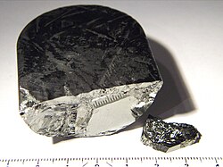
| Appearance | Dark grey, metallic crystals |
| Density | 5.7747 g⋅cm−3 [1] |
| Melting point | 524 °C (975 °F; 797 K) [1] |
| Band gap | 0.17 eV |
| Electron mobility | 7.7 mC⋅s⋅g−1 (at 27 °C) |
| Thermal conductivity | 180 mW⋅K−1⋅cm−1 (at 27 °C) |
Refractive index (nD) | 4 [2] |
| Structure | |
| Zincblende | |
| T2d-F-43m | |
a = 0.648 nm | |
| Tetrahedral | |
| Thermochemistry [3] | |
Heat capacity (C) | 49.5 J·K−1·mol−1 |
Std molar entropy (S⦵298) | 86.2 J·K−1·mol−1 |
Std enthalpy of formation (ΔfH⦵298) | −30.5 kJ·mol−1 |
Gibbs free energy (ΔfG⦵) | −25.5 kJ·mol−1 |
| Hazards | |
| GHS labelling: | |
  | |
| Warning | |
| H302, H332, H411 | |
| P273 | |
| Related compounds | |
Other anions | Indium nitride Indium phosphide Indium arsenide |
Except where otherwise noted, data are given for materials in their standard state (at 25 °C [77 °F], 100 kPa). | |
Indium antimonide (InSb) is a crystalline compound made from the elements indium (In) and antimony (Sb). It is a narrow-gap semiconductor material from the III-V group used in infrared detectors, including thermal imaging cameras, FLIR systems, infrared homing missile guidance systems, and in infrared astronomy. Indium antimonide detectors are sensitive to infrared wavelengths between 1 and 5 μm.
Contents
- History
- Physical properties
- Electronic properties
- Growth methods
- Device applications
- References
- Cited sources
- External links
Indium antimonide was a very common detector in the old, single-detector mechanically scanned thermal imaging systems. Another application is as a terahertz radiation source as it is a strong photo-Dember emitter.
