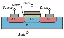
Cross-sectional view of a MOSFET type field-effect transistor, showing source, gate and drain terminals, and insulating oxide layer.
The field-effect transistor (FET) is a type of transistor that uses an electric field to control the current through a semiconductor. It comes in two types: junction FET (JFET) and metal-oxide-semiconductor FET (MOSFET). FETs have three terminals: source, gate, and drain. FETs control the current by the application of a voltage to the gate, which in turn alters the conductivity between the drain and source.
FETs are also known as unipolar transistors since they involve single-carrier-type operation. That is, FETs use either electrons (n-channel) or holes (p-channel) as charge carriers in their operation, but not both. Many different types of field effect transistors exist. Field effect transistors generally display very high input impedance at low frequencies. The most widely used field-effect transistor is the MOSFET (metal–oxide–semiconductor field-effect transistor).
The concept of a field-effect transistor (FET) was first patented by the Austro-Hungarian born physicist Julius Edgar Lilienfeld in 1925[1] and by Oskar Heil in 1934, but they were unable to build a working practical semiconducting device based on the concept. The transistor effect was later observed and explained by John Bardeen and Walter Houser Brattain while working under William Shockley at Bell Labs in 1947, shortly after the 17-year patent expired. Shockley initially attempted to build a working FET by trying to modulate the conductivity of a semiconductor, but was unsuccessful, mainly due to problems with the surface states, the dangling bond, and the germanium and copper compound materials. In the course of trying to understand the mysterious reasons behind their failure to build a working FET, it led to Bardeen and Brattain instead inventing the point-contact transistor in 1947, which was followed by Shockley's bipolar junction transistor in 1948.[2][3]
The first FET device to be successfully built was the junction field-effect transistor (JFET).[2] A JFET was first patented by Heinrich Welker in 1945.[4] The static induction transistor (SIT), a type of JFET with a short channel, was invented by Japanese engineers Jun-ichi Nishizawa and Y. Watanabe in 1950. Following Shockley's theoretical treatment on the JFET in 1952, a working practical JFET was built by George C. Dacey and Ian M. Ross in 1953.[5] However, the JFET still had issues affecting junction transistors in general.[6] Junction transistors were relatively bulky devices that were difficult to manufacture on a mass-production basis, which limited them to a number of specialised applications. The insulated-gate field-effect transistor (IGFET) was theorized as a potential alternative to junction transistors, but researchers were unable to build working IGFETs, largely due to the troublesome surface state barrier that prevented the external electric field from penetrating into the material.[6] By the mid-1950s, researchers had largely given up on the FET concept, and instead focused on bipolar junction transistor (BJT) technology.[7]
The foundations of MOSFET technology were laid down by the work of William Shockley, John Bardeen and Walter Brattain. Shockley independently envisioned the FET concept in 1945, but he was unable to build a working device. The next year Bardeen explained his failure in terms of surface states. Bardeen applied the theory of surface states on semiconductors (previous work on surface states was done by Shockley in 1939 and Igor Tamm in 1932) and realized that the external field was blocked at the surface because of extra electrons which are drawn to the semiconductor surface. Electrons become trapped in those localized states forming an inversion layer. Bardeen's hypothesis marked the birth of surface physics. Bardeen then decided to make use of an inversion layer instead of the very thin layer of semiconductor which Shockley had envisioned in his FET designs. Based on his theory, in 1948 Bardeen patented the progenitor of MOSFET, an insulated-gate FET (IGFET) with an inversion layer. The inversion layer confines the flow of minority carriers, increasing modulation and conductivity, although its electron transport depends on the gate's insulator or quality of oxide if used as an insulator, deposited above the inversion layer. Bardeen's patent as well as the concept of an inversion layer forms the basis of CMOS technology today. In 1976 Shockley described Bardeen's surface state hypothesis "as one of the most significant research ideas in the semiconductor program".[8]
After Bardeen's surface state theory the trio tried to overcome the effect of surface states. In late 1947, Robert Gibney and Brattain suggested the use of electrolyte placed between metal and semiconductor to overcome the effects of surface states. Their FET device worked, but amplification was poor. Bardeen went further and suggested to rather focus on the conductivity of the inversion layer. Further experiments led them to replace electrolyte with a solid oxide layer in the hope of getting better results. Their goal was to penetrate the oxide layer and get to the inversion layer. However, Bardeen suggested they switch from silicon to germanium and in the process their oxide got inadvertently washed off. They stumbled upon a completely different transistor, the point-contact transistor. Lillian Hoddeson argues that "had Brattain and Bardeen been working with silicon instead of germanium they would have stumbled across a successful field effect transistor".[8][9][10][11][12]
By the end of the first half of the 1950s, following theoretical and experimental work of Bardeen, Brattain, Kingston, Morrison and others, it became more clear that there were two types of surface states. Fast surface states were found to be associated with the bulk and a semiconductor/oxide interface. Slow surface states were found to be associated with the oxide layer because of adsorption of atoms, molecules and ions by the oxide from the ambient. The latter were found to be much more numerous and to have much longer relaxation times. At the time Philo Farnsworth and others came up with various methods of producing atomically clean semiconductor surfaces.
In 1955, Carl Frosch and Lincoln Derrick accidentally covered the surface of silicon wafer with a layer of silicon dioxide.[13] They showed that oxide layer prevented certain dopants into the silicon wafer, while allowing for others, thus discovering the passivating effect of oxidation on the semiconductor surface. Their further work demonstrated how to etch small openings in the oxide layer to diffuse dopants into selected areas of the silicon wafer. In 1957, they published a research paper and patented their technique summarizing their work. The technique they developed is known as oxide diffusion masking, which would later be used in the fabrication of MOSFET devices.[14] At Bell Labs, the importance of Frosch's technique was immediately realized. Results of their work circulated around Bell Labs in the form of BTL memos before being published in 1957. At Shockley Semiconductor, Shockley had circulated the preprint of their article in December 1956 to all his senior staff, including Jean Hoerni.[6][15][16]
In 1955, Ian Munro Ross filed a patent for a FeFET or MFSFET. Its structure was like that of a modern inversion channel MOSFET, but ferroelectric material was used as a dielectric/insulator instead of oxide. He envisioned it as a form of memory, years before the floating gate MOSFET. In February 1957, John Wallmark filed a patent for FET in which germanium monoxide was used as a gate dielectric, but he didn't pursue the idea. In his other patent filed the same year he described a double gate FET. In March 1957, in his laboratory notebook, Ernesto Labate, a research scientist at Bell Labs, conceived of a device similar to the later proposed MOSFET, although Labate's device didn't explicitly use silicon dioxide as an insulator.[17][18][19][20]
1957, Diagram of one of the SiO2 transistor devices made by Frosch and Derrick
In 1955, Carl Frosch and Lincoln Derrick accidentally grew a layer of silicon dioxide over the silicon wafer, for which they observed surface passivation effects.[21][22] By 1957 Frosch and Derrick, using masking and predeposition, were able to manufacture silicon dioxide transistors and showed that silicon dioxide insulated, protected silicon wafers and prevented dopants from diffusing into the wafer.[21][23] J.R. Ligenza and W.G. Spitzer studied the mechanism of thermally grown oxides and fabricated a high quality Si/SiO2 stack in 1960.[24][25][26]
Following this research, Mohamed Atalla and Dawon Kahng proposed a silicon MOS transistor in 1959[27] and successfully demonstrated a working MOS device with their Bell Labs team in 1960.[28][29] Their team included E. E. LaBate and E. I. Povilonis who fabricated the device; M. O. Thurston, L. A. D’Asaro, and J. R. Ligenza who developed the diffusion processes, and H. K. Gummel and R. Lindner who characterized the device.[30][31]
With its high scalability,[32] and much lower power consumption and higher density than bipolar junction transistors,[33] the MOSFET made it possible to build high-density integrated circuits.[34] The MOSFET is also capable of handling higher power than the JFET.[35] The MOSFET was the first truly compact transistor that could be miniaturised and mass-produced for a wide range of uses.[6] The MOSFET thus became the most common type of transistor in computers, electronics,[36] and communications technology (such as smartphones).[37] The US Patent and Trademark Office calls it a "groundbreaking invention that transformed life and culture around the world".[37]
FETs can be majority-charge-carrier devices, in which the current is carried predominantly by majority carriers, or minority-charge-carrier devices, in which the current is mainly due to a flow of minority carriers.[47] The device consists of an active channel through which charge carriers, electrons or holes, flow from the source to the drain. Source and drain terminal conductors are connected to the semiconductor through ohmic contacts. The conductivity of the channel is a function of the potential applied across the gate and source terminals.
source (S), through which the carriers enter the channel. Conventionally, current entering the channel at S is designated by IS.
drain (D), through which the carriers leave the channel. Conventionally, current leaving the channel at D is designated by ID. Drain-to-source voltage is VDS.
gate (G), the terminal that modulates the channel conductivity. By applying voltage to G, one can control ID.
More about terminals
Cross section of an n-type MOSFET
All FETs have source, drain, and gate terminals that correspond roughly to the emitter, collector, and base of BJTs. Most FETs have a fourth terminal called the body, base, bulk, or substrate. This fourth terminal serves to bias the transistor into operation; it is rare to make non-trivial use of the body terminal in circuit designs, but its presence is important when setting up the physical layout of an integrated circuit. The size of the gate, length L in the diagram, is the distance between source and drain. The width is the extension of the transistor, in the direction perpendicular to the cross section in the diagram (i.e., into/out of the screen). Typically the width is much larger than the length of the gate. A gate length of 1μm limits the upper frequency to about 5GHz, 0.2μm to about 30GHz.
The names of the terminals refer to their functions. The gate terminal may be thought of as controlling the opening and closing of a physical gate. This gate permits electrons to flow through or blocks their passage by creating or eliminating a channel between the source and drain. Electron-flow from the source terminal towards the drain terminal is influenced by an applied voltage. The body simply refers to the bulk of the semiconductor in which the gate, source and drain lie. Usually the body terminal is connected to the highest or lowest voltage within the circuit, depending on the type of the FET. The body terminal and the source terminal are sometimes connected together since the source is often connected to the highest or lowest voltage within the circuit, although there are several uses of FETs which do not have such a configuration, such as transmission gates and cascode circuits.
Unlike BJTs, the vast majority of FETs are electrically symmetrical. The source and drain terminals can thus be interchanged in practical circuits with no change in operating characteristics or function. This can be confusing when FET's appear to be connected "backwards" in schematic diagrams and circuits because the physical orientation of the FET was decided for other reasons, such as printed circuit layout considerations.
Effect of gate voltage on current
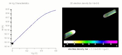
I–V characteristics and output plot of a JFET n-channel transistorSimulation result for right side: formation of inversion channel (electron density) and left side: current-gate voltage curve (transfer characteristics) in an n-channel nanowireMOSFET. Note that the threshold voltage for this device lies around 0.45V.FET conventional symbol types
The FET controls the flow of electrons (or electron holes) from the source to drain by affecting the size and shape of a "conductive channel" created and influenced by voltage (or lack of voltage) applied across the gate and source terminals. (For simplicity, this discussion assumes that the body and source are connected.) This conductive channel is the "stream" through which electrons flow from source to drain.
n-channel FET
In an n-channel "depletion-mode" device, a negative gate-to-source voltage causes a depletion region to expand in width and encroach on the channel from the sides, narrowing the channel. If the active region expands to completely close the channel, the resistance of the channel from source to drain becomes large, and the FET is effectively turned off like a switch (see right figure, when there is very small current). This is called "pinch-off", and the voltage at which it occurs is called the "pinch-off voltage". Conversely, a positive gate-to-source voltage increases the channel size and allows electrons to flow easily (see right figure, when there is a conduction channel and current is large).
In an n-channel "enhancement-mode" device, a conductive channel does not exist naturally within the transistor, and a positive gate-to-source voltage is necessary to create one. The positive voltage attracts free-floating electrons within the body towards the gate, forming a conductive channel. But first, enough electrons must be attracted near the gate to counter the dopant ions added to the body of the FET; this forms a region with no mobile carriers called a depletion region, and the voltage at which this occurs is referred to as the threshold voltage of the FET. Further gate-to-source voltage increase will attract even more electrons towards the gate which are able to create an active channel from source to drain; this process is called inversion.
p-channel FET
In a p-channel "depletion-mode" device, a positive voltage from gate to body widens the depletion layer by forcing electrons to the gate-insulator/semiconductor interface, leaving exposed a carrier-free region of immobile, positively charged acceptor ions.
Conversely, in a p-channel "enhancement-mode" device, a conductive region does not exist and negative voltage must be used to generate a conduction channel.
Effect of drain-to-source voltage on channel
For either enhancement- or depletion-mode devices, at drain-to-source voltages much less than gate-to-source voltages, changing the gate voltage will alter the channel resistance, and drain current will be proportional to drain voltage (referenced to source voltage). In this mode the FET operates like a variable resistor and the FET is said to be operating in a linear mode or ohmic mode.[49][50]
If drain-to-source voltage is increased, this creates a significant asymmetrical change in the shape of the channel due to a gradient of voltage potential from source to drain. The shape of the inversion region becomes "pinched-off" near the drain end of the channel. If drain-to-source voltage is increased further, the pinch-off point of the channel begins to move away from the drain towards the source. The FET is said to be in saturation mode;[51] although some authors refer to it as active mode, for a better analogy with bipolar transistor operating regions.[52][53] The saturation mode, or the region between ohmic and saturation, is used when amplification is needed. The in-between region is sometimes considered to be part of the ohmic or linear region, even where drain current is not approximately linear with drain voltage.
Even though the conductive channel formed by gate-to-source voltage no longer connects source to drain during saturation mode, carriers are not blocked from flowing. Considering again an n-channel enhancement-mode device, a depletion region exists in the p-type body, surrounding the conductive channel and drain and source regions. The electrons which comprise the channel are free to move out of the channel through the depletion region if attracted to the drain by drain-to-source voltage. The depletion region is free of carriers and has a resistance similar to silicon. Any increase of the drain-to-source voltage will increase the distance from drain to the pinch-off point, increasing the resistance of the depletion region in proportion to the drain-to-source voltage applied. This proportional change causes the drain-to-source current to remain relatively fixed, independent of changes to the drain-to-source voltage, quite unlike its ohmic behavior in the linear mode of operation. Thus, in saturation mode, the FET behaves as a constant-current source rather than as a resistor, and can effectively be used as a voltage amplifier. In this case, the gate-to-source voltage determines the level of constant current through the channel.
Among the more unusual body materials are amorphous silicon, polycrystalline silicon or other amorphous semiconductors in thin-film transistors or organic field-effect transistors (OFETs) that are based on organic semiconductors; often, OFET gate insulators and electrodes are made of organic materials, as well. Such FETs are manufactured using a variety of materials such as silicon carbide (SiC), gallium arsenide (GaAs), gallium nitride (GaN), and indium gallium arsenide (InGaAs).
In June 2011, IBM announced that it had successfully used graphene-based FETs in an integrated circuit.[54][55] These transistors are capable of about 2.23GHz cutoff frequency, much higher than standard silicon FETs.[56]
Top: source, bottom: drain, left: gate, right: bulk. Voltages that lead to channel formation are not shown.
The channel of a FET is doped to produce either an n-type semiconductor or a p-type semiconductor. The drain and source may be doped of opposite type to the channel, in the case of enhancement mode FETs, or doped of similar type to the channel as in depletion mode FETs. Field-effect transistors are also distinguished by the method of insulation between channel and gate. Types of FETs include:
The MOSFET (metal–oxide–semiconductor field-effect transistor) utilizes an insulator (typically SiO2) between the gate and the body. This is by far the most common type of FET.
The DGMOSFET (dual-gate MOSFET) or DGMOS, a MOSFET with two insulated gates.
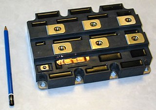
The IGBT (insulated-gate bipolar transistor) is a device for power control. It has a structure akin to a MOSFET coupled with a bipolar-like main conduction channel. These are commonly used for the 200–3000 V drain-to-source voltage range of operation. Power MOSFETs are still the device of choice for drain-to-source voltages of 1 to 200 V.
The JLNT (Junctionless nanowire transistor) is a type of Field-effect transistor (FET) which channel is one or multiple nanowires and does not present any junction.
The ISFET (ion-sensitive field-effect transistor) can be used to measure ion concentrations in a solution; when the ion concentration (such as H+, see pH electrode) changes, the current through the transistor will change accordingly.
The BioFET (Biologically sensitive field-effect transistor) is a class of sensors/biosensors based on ISFET technology which are utilized to detect charged molecules; when a charged molecule is present, changes in the electrostatic field at the BioFET surface result in a measurable change in current through the transistor. These include enzyme modified FETs (EnFETs), immunologically modified FETs (ImmunoFETs), gene-modified FETs (GenFETs), DNAFETs, cell-based BioFETs (CPFETs), beetle/chip FETs (BeetleFETs), and FETs based on ion-channels/protein binding.[57]
The DNAFET (DNA field-effect transistor) is a specialized FET that acts as a biosensor, by using a gate made of single-strand DNA molecules to detect matching DNA strands.
finFET, including GAAFET or gate-all-around FET, used on high density processor chips
The JFET (junction field-effect transistor) uses a reverse biased p–n junction to separate the gate from the body.
The DEPFET is a FET formed in a fully depleted substrate and acts as a sensor, amplifier and memory node at the same time. It can be used as an image (photon) sensor.
The FREDFET (fast-reverse or fast-recovery epitaxial diode FET) is a specialized FET designed to provide a very fast recovery (turn-off) of the body diode, making it convenient for driving inductive loads such as electric motors, especially medium-powered brushless DC motors.
The HIGFET (heterostructure insulated-gate field-effect transistor) is now used mainly in research.[58]
The TQFET (topological quantum field-effect transistor) switches a 2D material from dissipationless topological insulator ('on' state) to conventional insulator ('off' state) using an applied electric field.[60]
The HEMT (high-electron-mobility transistor), also called a HFET (heterostructure FET), can be made using bandgap engineering in a ternary semiconductor such as AlGaAs. The fully depleted wide-band-gap material forms the isolation between gate and body.
The GNRFET (graphene nanoribbon field-effect transistor) uses a graphene nanoribbon for its channel.[62]
The VeSFET (vertical-slit field-effect transistor) is a square-shaped junctionless FET with a narrow slit connecting the source and drain at opposite corners. Two gates occupy the other corners, and control the current through the slit.[63]
The QFET (quantum field effect transistor) takes advantage of quantum tunneling to greatly increase the speed of transistor operation by eliminating the traditional transistor's area of electron conduction.
The SB-FET (Schottky-barrier field-effect transistor) is a field-effect transistor with metallic source and drain contact electrodes, which create Schottky barriers at both the source-channel and drain-channel interfaces.[64][65]
The GFET is a highly sensitive graphene-based field effect transistor used as biosensors and chemical sensors. Due to the 2 dimensional structure of graphene, along with its physical properties, GFETs offer increased sensitivity, and reduced instances of 'false positives' in sensing applications[66]
The Fe FET uses a ferroelectric between the gate, allowing the transistor to retain its state in the absence of bias - such devices may have application as non-volatile memory.
Field-effect transistors have high gate-to-drain current resistance, of the order of 100 MΩ or more, providing a high degree of isolation between control and flow. Because base current noise will increase with shaping time[clarification needed],[68] a FET typically produces less noise than a bipolar junction transistor (BJT), and is found in noise-sensitive electronics such as tuners and low-noise amplifiers for VHF and satellite receivers. It exhibits no offset voltage at zero drain current and makes an excellent signal chopper. It typically has better thermal stability than a BJT.[48]
Because the FETs are controlled by gate charge, once the gate is closed or open, there is no additional power draw, as there would be with a bipolar junction transistor or with non-latching relays in some states. This allows extremely low-power switching, which in turn allows greater miniaturization of circuits because heat dissipation needs are reduced compared to other types of switches.
Disadvantages
A field-effect transistor has a relatively low gain–bandwidth product compared to a bipolar junction transistor. MOSFETs are very susceptible to overload voltages, thus requiring special handling during installation.[69] The fragile insulating layer of the MOSFET between the gate and the channel makes it vulnerable to electrostatic discharge or changes to threshold voltage during handling. This is not usually a problem after the device has been installed in a properly designed circuit.
FETs often have a very low "on" resistance and have a high "off" resistance. However, the intermediate resistances are significant, and so FETs can dissipate large amounts of power while switching. Thus, efficiency can put a premium on switching quickly, but this can cause transients that can excite stray inductances and generate significant voltages that can couple to the gate and cause unintentional switching. FET circuits can therefore require very careful layout and can involve trades between switching speed and power dissipation. There is also a trade-off between voltage rating and "on" resistance, so high-voltage FETs have a relatively high "on" resistance and hence conduction losses.[70]
Failure modes
Field-effect transistors are relatively robust, especially when operated within the temperature and electrical limitations defined by the manufacturer (proper derating). However, modern FET devices can often incorporate a body diode. If the characteristics of the body diode are not taken into consideration, the FET can experience slow body diode behavior, where a parasitic transistor will turn on and allow high current to be drawn from drain to source when the FET is off.[71]
The most commonly used FET is the MOSFET. The CMOS (complementary metal oxide semiconductor) process technology is the basis for modern digitalintegrated circuits. This process technology uses an arrangement where the (usually "enhancement-mode") p-channel MOSFET and n-channel MOSFET are connected in series such that when one is on, the other is off.
In FETs, electrons can flow in either direction through the channel when operated in the linear mode. The naming convention of drain terminal and source terminal is somewhat arbitrary, as the devices are typically (but not always) built symmetrical from source to drain. This makes FETs suitable for switching analog signals between paths (multiplexing). With this concept, one can construct a solid-state mixing board, for example. FET is commonly used as an amplifier. For example, due to its large input resistance and low output resistance, it is effective as a buffer in common-drain (source follower) configuration.
IGBTs are used in switching internal combustion engine ignition coils, where fast switching and voltage blocking capabilities are important.
Source-gated transistor
Source-gated transistors are more robust to manufacturing and environmental issues in large-area electronics such as display screens, but are slower in operation than FETs.[72]
A transistor is a semiconductor device used to amplify or switch electrical signals and power. It is one of the basic building blocks of modern electronics. It is composed of semiconductor material, usually with at least three terminals for connection to an electronic circuit. A voltage or current applied to one pair of the transistor's terminals controls the current through another pair of terminals. Because the controlled (output) power can be higher than the controlling (input) power, a transistor can amplify a signal. Some transistors are packaged individually, but many more in miniature form are found embedded in integrated circuits. Because transistors are the key active components in practically all modern electronics, many people consider them one of the 20th century's greatest inventions.
A semiconductor device is an electronic component that relies on the electronic properties of a semiconductor material for its function. Its conductivity lies between conductors and insulators. Semiconductor devices have replaced vacuum tubes in most applications. They conduct electric current in the solid state, rather than as free electrons across a vacuum or as free electrons and ions through an ionized gas.
In electronics, the metal–oxide–semiconductor field-effect transistor is a type of field-effect transistor (FET), most commonly fabricated by the controlled oxidation of silicon. It has an insulated gate, the voltage of which determines the conductivity of the device. This ability to change conductivity with the amount of applied voltage can be used for amplifying or switching electronic signals. The term metal–insulator–semiconductor field-effect transistor (MISFET) is almost synonymous with MOSFET. Another near-synonym is insulated-gate field-effect transistor (IGFET).
The junction field-effect transistor (JFET) is one of the simplest types of field-effect transistor. JFETs are three-terminal semiconductor devices that can be used as electronically controlled switches or resistors, or to build amplifiers.
NMOS or nMOS logic uses n-type (-) MOSFETs to implement logic gates and other digital circuits.
Complementary metal–oxide–semiconductor is a type of metal–oxide–semiconductor field-effect transistor (MOSFET) fabrication process that uses complementary and symmetrical pairs of p-type and n-type MOSFETs for logic functions. CMOS technology is used for constructing integrated circuit (IC) chips, including microprocessors, microcontrollers, memory chips, and other digital logic circuits. CMOS technology is also used for analog circuits such as image sensors, data converters, RF circuits, and highly integrated transceivers for many types of communication.
An insulated-gate bipolar transistor (IGBT) is a three-terminal power semiconductor device primarily forming an electronic switch. It was developed to combine high efficiency with fast switching. It consists of four alternating layers (NPNP) that are controlled by a metal–oxide–semiconductor (MOS) gate structure.
A MESFET is a field-effect transistor semiconductor device similar to a JFET with a Schottky (metal–semiconductor) junction instead of a p–n junction for a gate.
The threshold voltage, commonly abbreviated as Vth or VGS(th), of a field-effect transistor (FET) is the minimum gate-to-source voltage (VGS) that is needed to create a conducting path between the source and drain terminals. It is an important scaling factor to maintain power efficiency.
An organic field-effect transistor (OFET) is a field-effect transistor using an organic semiconductor in its channel. OFETs can be prepared either by vacuum evaporation of small molecules, by solution-casting of polymers or small molecules, or by mechanical transfer of a peeled single-crystalline organic layer onto a substrate. These devices have been developed to realize low-cost, large-area electronic products and biodegradable electronics. OFETs have been fabricated with various device geometries. The most commonly used device geometry is bottom gate with top drain and source electrodes, because this geometry is similar to the thin-film silicon transistor (TFT) using thermally grown SiO2 as gate dielectric. Organic polymers, such as poly(methyl-methacrylate) (PMMA), can also be used as dielectric. One of the benefits of OFETs, especially compared with inorganic TFTs, is their unprecedented physical flexibility, which leads to biocompatible applications, for instance in the future health care industry of personalized biomedicines and bioelectronics.
A power MOSFET is a specific type of metal–oxide–semiconductor field-effect transistor (MOSFET) designed to handle significant power levels. Compared to the other power semiconductor devices, such as an insulated-gate bipolar transistor (IGBT) or a thyristor, its main advantages are high switching speed and good efficiency at low voltages. It shares with the IGBT an isolated gate that makes it easy to drive. They can be subject to low gain, sometimes to a degree that the gate voltage needs to be higher than the voltage under control.
A VMOS transistor is a type of metal–oxide–semiconductor field-effect transistor (MOSFET). VMOS is also used to describe the V-groove shape vertically cut into the substrate material.
In semiconductor electronics fabrication technology, a self-aligned gate is a transistor manufacturing approach whereby the gate electrode of a MOSFET is used as a mask for the doping of the source and drain regions. This technique ensures that the gate is naturally and precisely aligned to the edges of the source and drain.
A multigate device, multi-gate MOSFET or multi-gate field-effect transistor (MuGFET) refers to a metal–oxide–semiconductor field-effect transistor (MOSFET) that has more than one gate on a single transistor. The multiple gates may be controlled by a single gate electrode, wherein the multiple gate surfaces act electrically as a single gate, or by independent gate electrodes. A multigate device employing independent gate electrodes is sometimes called a multiple-independent-gate field-effect transistor (MIGFET). The most widely used multi-gate devices are the FinFET and the GAAFET, which are non-planar transistors, or 3D transistors.
PMOS or pMOS logic is a family of digital circuits based on p-channel, enhancement mode metal–oxide–semiconductor field-effect transistors (MOSFETs). In the late 1960s and early 1970s, PMOS logic was the dominant semiconductor technology for large-scale integrated circuits before being superseded by NMOS and CMOS devices.
A transistor is a semiconductor device with at least three terminals for connection to an electric circuit. In the common case, the third terminal controls the flow of current between the other two terminals. This can be used for amplification, as in the case of a radio receiver, or for rapid switching, as in the case of digital circuits. The transistor replaced the vacuum-tube triode, also called a (thermionic) valve, which was much larger in size and used significantly more power to operate. The first transistor was successfully demonstrated on December 23, 1947, at Bell Laboratories in Murray Hill, New Jersey. Bell Labs was the research arm of American Telephone and Telegraph (AT&T). The three individuals credited with the invention of the transistor were William Shockley, John Bardeen and Walter Brattain. The introduction of the transistor is often considered one of the most important inventions in history.
The gate oxide is the dielectric layer that separates the gate terminal of a MOSFET from the underlying source and drain terminals as well as the conductive channel that connects source and drain when the transistor is turned on. Gate oxide is formed by thermal oxidation of the silicon of the channel to form a thin insulating layer of silicon dioxide. The insulating silicon dioxide layer is formed through a process of self-limiting oxidation, which is described by the Deal–Grove model. A conductive gate material is subsequently deposited over the gate oxide to form the transistor. The gate oxide serves as the dielectric layer so that the gate can sustain as high as 1 to 5 MV/cm transverse electric field in order to strongly modulate the conductance of the channel.
In field-effect transistors (FETs), depletion mode and enhancement mode are two major transistor types, corresponding to whether the transistor is in an on state or an off state at zero gate–source voltage.
Polysilicon depletion effect is the phenomenon in which unwanted variation of threshold voltage of the MOSFET devices using polysilicon as gate material is observed, leading to unpredicted behavior of the electronic circuit. Because of this variation High-k Dielectric Metal Gates (HKMG) were introduced to solve the issue.
A FET amplifier is an amplifier that uses one or more field-effect transistors (FETs). The most common type of FET amplifier is the MOSFET amplifier, which uses metal–oxide–semiconductor FETs (MOSFETs). The main advantage of a FET used for amplification is that it has very high input impedance and low output impedance.
↑ Lillian Hoddeson (1994). "Research on crystal rectifiers during World War II and the invention of the transistor". History and Technology. 11 (2): 121–130. doi:10.1080/07341519408581858.
↑ Michael Riordan; Lillian Hoddeson (1997). Crystal Fire: The Birth of the Information Age. W. W. Norton & Company. ISBN978-0-393-04124-8.
↑ US2802760A,Lincoln, Derick&Frosch, Carl J.,"Oxidation of semiconductive surfaces for controlled diffusion",issued 1957-08-13
↑ Lojek, Bo (2007). History of Semiconductor Engineering. Springer Science & Business Media. p.324. ISBN978-3-540-34258-8.
↑ Stefan Ferdinand Müller (2016). Development of HfO2-Based Ferroelectric Memories for Future CMOS Technology Nodes. BoD – Books on Demand. ISBN978-3-7392-4894-3.
↑ D. Kahng and S. M. Sze, "A floating gate and its application to memory devices", The Bell System Technical Journal, vol. 46, no. 4, 1967, pp. 1288–1295
↑ PR Gray; PJ Hurst; SH Lewis; RG Meyer (2001). Analysis and design of analog integrated circuits (Fourthed.). New York: Wiley. pp.§1.5.2 p. 45. ISBN978-0-471-32168-2.
↑ Sarvari H.; Ghayour, R.; Dastjerdy, E. (2011). "Frequency analysis of graphene nanoribbon FET by Non-Equilibrium Green's Function in mode space". Physica E: Low-dimensional Systems and Nanostructures. 43 (8): 1509–1513. Bibcode:2011PhyE...43.1509S. doi:10.1016/j.physe.2011.04.018.
This page is based on this Wikipedia article Text is available under the CC BY-SA 4.0 license; additional terms may apply. Images, videos and audio are available under their respective licenses.