
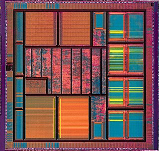
An integrated circuit, also known as a microchip, chip or IC, is a small electronic device made up of multiple interconnected electronic components such as transistors, resistors, and capacitors. These components are etched onto a small piece of semiconductor material, usually silicon. Integrated circuits are used in a wide range of electronic devices, including computers, smartphones, and televisions, to perform various functions such as processing and storing information. They have greatly impacted the field of electronics by enabling device miniaturization and enhanced functionality.

Semiconductor device fabrication is the process used to manufacture semiconductor devices, typically integrated circuits (ICs) such as computer processors, microcontrollers, and memory chips that are present in everyday electronic devices. It is a multiple-step photolithographic and physio-chemical process during which electronic circuits are gradually created on a wafer, typically made of pure single-crystal semiconducting material. Silicon is almost always used, but various compound semiconductors are used for specialized applications.
In electronics and photonics design, tape-out or tapeout is the final result of the design process for integrated circuits or printed circuit boards before they are sent for manufacturing. The tapeout is specifically the point at which the graphic for the photomask of the circuit is sent to the fabrication facility.
Very-large-scale integration (VLSI) is the process of creating an integrated circuit (IC) by combining millions or billions of MOS transistors onto a single chip. VLSI began in the 1970s when MOS integrated circuit chips were developed and then widely adopted, enabling complex semiconductor and telecommunication technologies. The microprocessor and memory chips are VLSI devices.

An application-specific integrated circuit is an integrated circuit (IC) chip customized for a particular use, rather than intended for general-purpose use, such as a chip designed to run in a digital voice recorder or a high-efficiency video codec. Application-specific standard product chips are intermediate between ASICs and industry standard integrated circuits like the 7400 series or the 4000 series. ASIC chips are typically fabricated using metal–oxide–semiconductor (MOS) technology, as MOS integrated circuit chips.
Electronic design automation (EDA), also referred to as electronic computer-aided design (ECAD), is a category of software tools for designing electronic systems such as integrated circuits and printed circuit boards. The tools work together in a design flow that chip designers use to design and analyze entire semiconductor chips. Since a modern semiconductor chip can have billions of components, EDA tools are essential for their design; this article in particular describes EDA specifically with respect to integrated circuits (ICs).

GDSII stream format (GDSII), is a binary database file format which is the de facto industry standard for Electronic Design Automation data exchange of integrated circuit or IC layout artwork. It is a binary file format representing planar geometric shapes, text labels, and other information about the layout in hierarchical form. The data can be used to reconstruct all or part of the artwork to be used in sharing layouts, transferring artwork between different tools, or creating photomasks.
Place and route is a stage in the design of printed circuit boards, integrated circuits, and field-programmable gate arrays. As implied by the name, it is composed of two steps, placement and routing. The first step, placement, involves deciding where to place all electronic components, circuitry, and logic elements in a generally limited amount of space. This is followed by routing, which decides the exact design of all the wires needed to connect the placed components. This step must implement all the desired connections while following the rules and limitations of the manufacturing process.
A mixed-signal integrated circuit is any integrated circuit that has both analog circuits and digital circuits on a single semiconductor die. Their usage has grown dramatically with the increased use of cell phones, telecommunications, portable electronics, and automobiles with electronics and digital sensors.
In electronic design automation, a design rule is a geometric constraint imposed on circuit board, semiconductor device, and integrated circuit (IC) designers to ensure their designs function properly, reliably, and can be produced with acceptable yield. Design rules for production are developed by process engineers based on the capability of their processes to realize design intent. Electronic design automation is used extensively to ensure that designers do not violate design rules; a process called design rule checking (DRC). DRC is a major step during physical verification signoff on the design, which also involves LVS checks, XOR checks, ERC, and antenna checks. The importance of design rules and DRC is greatest for ICs, which have micro- or nano-scale geometries; for advanced processes, some fabs also insist upon the use of more restricted rules to improve yield.
In semiconductor design, standard-cell methodology is a method of designing application-specific integrated circuits (ASICs) with mostly digital-logic features. Standard-cell methodology is an example of design abstraction, whereby a low-level very-large-scale integration (VLSI) layout is encapsulated into an abstract logic representation.

The front end of line (FEOL) is the first portion of IC fabrication where the individual components are patterned in the semiconductor. FEOL generally covers everything up to the deposition of metal interconnect layers.
While the term front end of line (FEOL) refers to the first portion of any IC fabrication where the individual devices are patterned in the semiconductor, back end of line (BEOL) comprises the subsequent deposition of metal interconnect layers. Thus, BEOL is the second portion of IC fabrication process where the individual devices get interconnected with wiring by deposited metalization layers.

Integrated circuit design, semiconductor design, chip design or IC design, is a sub-field of electronics engineering, encompassing the particular logic and circuit design techniques required to design integrated circuits, or ICs. ICs consist of miniaturized electronic components built into an electrical network on a monolithic semiconductor substrate by photolithography.
Mask data preparation (MDP), also known as layout post processing, is the procedure of translating a file containing the intended set of polygons from an integrated circuit layout into set of instructions that a photomask writer can use to generate a physical mask. Typically, amendments and additions to the chip layout are performed in order to convert the physical layout into data for mask production.
Physical verification is a process whereby an integrated circuit layout design is verified via EDA software tools to ensure correct electrical and logical functionality and manufacturability. Verification involves design rule check (DRC), layout versus schematic (LVS), XOR, antenna checks and electrical rule check (ERC).

Multi-project chip (MPC), and multi-project wafer (MPW) semiconductor manufacturing arrangements allow customers to share tooling and microelectronics wafer fabrication cost between several designs or projects.

In integrated circuit design, physical design is a step in the standard design cycle which follows after the circuit design. At this step, circuit representations of the components of the design are converted into geometric representations of shapes which, when manufactured in the corresponding layers of materials, will ensure the required functioning of the components. This geometric representation is called integrated circuit layout. This step is usually split into several sub-steps, which include both design and verification and validation of the layout.

In electronic design automation, a floorplan of an integrated circuit is a schematic representation of tentative placement of its major functional blocks.
In the automated design of integrated circuits, signoff checks is the collective name given to a series of verification steps that the design must pass before it can be taped out. This implies an iterative process involving incremental fixes across the board using one or more check types, and then retesting the design. There are two types of sign-off's: front-end sign-off and back-end sign-off. After back-end sign-off, the chip goes to fabrication. After listing out all the features in the specification, the verification engineer will write coverage for those features to identify bugs, and send back the RTL design to the designer. Bugs, or defects, can include issues like missing features, errors in design, etc. When the coverage reaches a maximum percentage then the verification team will sign it off. By using a methodology like UVM, OVM, or VMM, the verification team develops a reusable environment. Nowadays, UVM is more popular than others.
