Related Research Articles
In electronics and photonics design, tape-out or tapeout is the final result of the design process for integrated circuits or printed circuit boards before they are sent for manufacturing. The tapeout is specifically the point at which the graphic for the photomask of the circuit is sent to the fabrication facility.
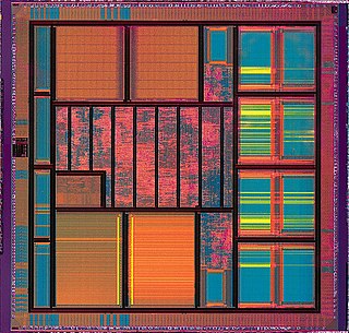
Very-large-scale integration (VLSI) is the process of creating an integrated circuit (IC) by combining millions or billions of MOS transistors onto a single chip. VLSI began in the 1970s when MOS integrated circuit chips were developed and then widely adopted, enabling complex semiconductor and telecommunication technologies. The microprocessor and memory chips are VLSI devices.

A printed circuit board (PCB), also called printed wiring board (PWB), is a medium used to connect or "wire" components to one another in a circuit. It takes the form of a laminated sandwich structure of conductive and insulating layers: each of the conductive layers is designed with a pattern of traces, planes and other features etched from one or more sheet layers of copper laminated onto and/or between sheet layers of a non-conductive substrate. Electrical components may be fixed to conductive pads on the outer layers in the shape designed to accept the component's terminals, generally by means of soldering, to both electrically connect and mechanically fasten them to it. Another manufacturing process adds vias, plated-through holes that allow interconnections between layers.
In computer engineering, a hardware description language (HDL) is a specialized computer language used to describe the structure and behavior of electronic circuits, most commonly to design ASICs and program FPGAs.

An application-specific integrated circuit is an integrated circuit (IC) chip customized for a particular use, rather than intended for general-purpose use, such as a chip designed to run in a digital voice recorder or a high-efficiency video codec. Application-specific standard product chips are intermediate between ASICs and industry standard integrated circuits like the 7400 series or the 4000 series. ASIC chips are typically fabricated using metal–oxide–semiconductor (MOS) technology, as MOS integrated circuit chips.
Electronic design automation (EDA), also referred to as electronic computer-aided design (ECAD), is a category of software tools for designing electronic systems such as integrated circuits and printed circuit boards. The tools work together in a design flow that chip designers use to design and analyze entire semiconductor chips. Since a modern semiconductor chip can have billions of components, EDA tools are essential for their design; this article in particular describes EDA specifically with respect to integrated circuits (ICs).
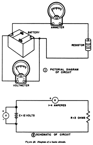
A circuit diagram is a graphical representation of an electrical circuit. A pictorial circuit diagram uses simple images of components, while a schematic diagram shows the components and interconnections of the circuit using standardized symbolic representations. The presentation of the interconnections between circuit components in the schematic diagram does not necessarily correspond to the physical arrangements in the finished device.

In integrated circuit design, integrated circuit (IC) layout, also known IC mask layout or mask design, is the representation of an integrated circuit in terms of planar geometric shapes which correspond to the patterns of metal, oxide, or semiconductor layers that make up the components of the integrated circuit. Originally the overall process was called tapeout, as historically early ICs used graphical black crepe tape on mylar media for photo imaging.
A silicon compiler is an electronic design automation software tool that is used for high-level synthesis of integrated circuits. Such tool takes a user's specification of an IC design as input and automatically generates an integrated circuit (IC) design files as output for further fabrication by the seminconductor fabrication plant or manually from discrete components. The process is sometimes referred to as hardware compilation. The silicon compiler may use vendor's Process Design Kit for the production.

In semiconductor design, standard-cell methodology is a method of designing application-specific integrated circuits (ASICs) with mostly digital-logic features. Standard-cell methodology is an example of design abstraction, whereby a low-level very-large-scale integration (VLSI) layout is encapsulated into an abstract logic representation.

OrCAD Systems Corporation was a software company that made OrCAD, a proprietary software tool suite used primarily for electronic design automation (EDA). The software is used mainly by electronic design engineers and electronic technicians to create electronic schematics, and perform mixed-signal simulation and electronic prints for manufacturing printed circuit boards (PCBs). OrCAD was taken over by Cadence Design Systems in 1999 and was integrated with Cadence Allegro in 2005.

The front end of line (FEOL) is the first portion of IC fabrication where the individual components are patterned in the semiconductor. FEOL generally covers everything up to the deposition of metal interconnect layers.
While the term front end of line (FEOL) refers to the first portion of any IC fabrication where the individual devices are patterned in the semiconductor, back end of line (BEOL) comprises the subsequent deposition of metal interconnect layers. Thus, BEOL is the second portion of IC fabrication process where the individual devices get interconnected with wiring by deposited metalization layers.
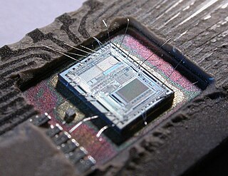
Integrated circuit design, or IC design, is a sub-field of electronics engineering, encompassing the particular logic and circuit design techniques required to design integrated circuits, or ICs. ICs consist of miniaturized electronic components built into an electrical network on a monolithic semiconductor substrate by photolithography.
Placement is an essential step in electronic design automation — the portion of the physical design flow that assigns exact locations for various circuit components within the chip's core area. An inferior placement assignment will not only affect the chip's performance but might also make it non-manufacturable by producing excessive wire-length, which is beyond available routing resources. Consequently, a placer must perform the assignment while optimizing a number of objectives to ensure that a circuit meets its performance demands. Together, the placement and routing steps of IC design are known as place and route.

The Layout Versus Schematic (LVS) is the class of electronic design automation (EDA) verification software that determines whether a particular integrated circuit layout corresponds to the original schematic or circuit diagram of the design.
An electronic circuit is composed of individual electronic components, such as resistors, transistors, capacitors, inductors and diodes, connected by conductive wires or traces through which electric current can flow. It is a type of electrical circuit. For a circuit to be referred to as electronic, rather than electrical, generally at least one active component must be present. The combination of components and wires allows various simple and complex operations to be performed: signals can be amplified, computations can be performed, and data can be moved from one place to another.

In integrated circuit design, physical design is a step in the standard design cycle which follows after the circuit design. At this step, circuit representations of the components of the design are converted into geometric representations of shapes which, when manufactured in the corresponding layers of materials, will ensure the required functioning of the components. This geometric representation is called integrated circuit layout. This step is usually split into several sub-steps, which include both design and verification and validation of the layout.

In electronic design automation, a floorplan of an integrated circuit is a schematic representation of tentative placement of its major functional blocks.
This page is a comparison of electronic design automation (EDA) software which is used today to design the near totality of electronic devices. Modern electronic devices are too complex to be designed without the help of a computer. Electronic devices may consist of integrated circuits (ICs), printed circuit boards (PCBs), field-programmable gate arrays (FPGAs) or a combination of them. Integrated circuits may consist of a combination of digital and analog circuits. These circuits can contain a combination of transistors, resistors, capacitors or specialized components such as analog neural networks, antennas or fuses.
References
- 1 2 J. Lienig, J. Scheible (2020). "Chap. 1.3.3: Physical Design of Printed Circuit Boards". Fundamentals of Layout Design for Electronic Circuits. Springer. p. 26-27. doi:10.1007/978-3-030-39284-0. ISBN 978-3-030-39284-0. S2CID 215840278.
- 1 2 "FPGA/PCB Co-Design Increases Fabrication Yields". Printed Circuit Design and Fabrication. Retrieved 2008-07-24.
- ↑ A. Kahng, J. Lienig, I. Markov, J. Hu: "VLSI Physical Design: From Graph Partitioning to Timing Closure", Springer (2022), doi : 10.1007/978-3-030-96415-3, ISBN 978-3-030-96414-6, pp. 5-10.