In electronic design, wire routing, commonly called simply routing, is a step in the design of printed circuit boards (PCBs) and integrated circuits (ICs). It builds on a preceding step, called placement, which determines the location of each active element of an IC or component on a PCB. After placement, the routing step adds wires needed to properly connect the placed components while obeying all design rules for the IC. Together, the placement and routing steps of IC design are known as place and route.
The task of all routers is the same. They are given some pre-existing polygons consisting of pins (also called terminals) on cells, some obstacles where wires cannot be routed, and optionally some pre-existing wiring called preroutes. Each of the pins is associated with a net, usually by name or number. The primary task of the router is to create geometries such that all terminals assigned to the same net are connected, no terminals assigned to different nets are connected, and all design rules are obeyed. A router can fail by not connecting terminals that should be connected (an open), by mistakenly connecting two terminals that should not be connected (a short), or by creating a design rule violation. In addition to correctly connecting the nets, routers may also be expected to make sure the design meets timing, has no crosstalk problems, meets any metal density requirements, does not suffer from antenna effects, and so on. This long list of often conflicting objectives is what makes routing extremely difficult.
Complexity of routing
Almost every problem associated with routing is known to be intractable. The simplest routing problem, called the Steiner tree problem, of finding the shortest route for one net in one layer with no obstacles and no design rules is known to be NP-complete, both in the case where all angles are allowed or if routing is restricted to only horizontal and vertical wires.[1] Variants of channel routing have also been shown to be NP-complete,[2] as well as routing which reduces crosstalk, number of vias, and so on. Even before routing problems were proved NP-complete, the difficulty of finding optimal solutions was apparent. Therefore almost all algorithms are based on heuristics, which do not try for an optimum, but instead a solution that is "good enough".[3]
Design rules sometimes vary considerably from layer to layer. On integrated circuits with multiple metal layers, for example, the allowed width and spacing on the lower layers may be four or more times smaller than the allowed widths and spacings on the upper layers. This introduces many additional complications not faced by routers for other applications such as printed circuit board or multi-chip module design. Particular difficulties ensue if the rules are not simple multiples of each other, and when vias must traverse between layers with different rules.
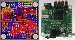
A PCB as a design on a computer (left) and realized as a board assembly populated with components (right). The board is double sided, with through-hole plating, green solder resist and a white legend. Both surface mount and through-hole components have been used.
Overall routing strategy
The earliest types of EDA routers were "manual routers"—the drafter clicked a mouse on the endpoint of each line segment of each net. Modern PCB design software typically provides "interactive routers"—the drafter selects a pad and clicks a few places to give the EDA tool an idea of where to go, and the EDA tool tries to place wires as close to that path as possible without violating design rule checking (DRC). Some more advanced interactive routers have "push and shove" (aka "shove-aside" or "automoving") features in an interactive router; the EDA tool pushes other nets out of the way, if possible, in order to place a new wire where the drafter wants it and still avoid violating DRC. Modern PCB design software also typically provides "autorouters" that route all remaining unrouted connections without human intervention.
Modern integrated circuits typically use fully automatic routing, as there can be far too many nets to route by hand. If the automatic routing does not yield a fully routed solution, a typical fix is to change the placement to allow more room for the routes, rather than try to complete the missing routes manually.
SimplifyPCB (a topological router with a focus on bundle routing with hand-routing results)[21]
How routers work
Many routers execute the following overall algorithm:
First, determine an approximate course for each net, often by routing on a coarse grid. This step is called global routing,[22] and may optionally include layer assignment. Global routing limits the size and complexity of the following detailed routing steps, which can be done grid square by grid square.
For detailed routing, the most common technique is rip-up and reroute aka rip-up and retry:[4]
Select a sequence in which the nets are to be routed.
Route each net in sequence
If not all nets can be successfully routed, apply any of a variety of "cleanup" methods, in which selected routings are removed, the order of the remaining nets to be routed is changed, and the remaining routings are attempted again.
This process repeats until all nets are routed or the program (or user) gives up.
An alternative approach is to treat shorts, design rule violations, obstructions, etc. on a similar footing as excess wire length—that is, as finite costs to be reduced (at first) rather than as absolutes to be avoided. This multi-pass "iterative-improvement" routing method[23] is described by the following algorithm:
For each of several iterative passes:
Prescribe or adjust the weight parameters of an "objective function" (having a weight parameter value for each unit of excess wire length, and for each type of violation). E.g., for the first pass, excess wire length may typically be given a high cost, while design violations such as shorts, adjacency, etc. are given a low cost. In later passes, the relative ordering of costs is changed so that violations are high-cost, or may be prohibited absolutely.
Select (or randomly choose) a sequence in which nets are to be routed during this pass.
"Rip up" (if previously routed) and reroute each net in turn, so as to minimize the value of the objective function for that net. (Some of the routings will in general have shorts or other design violations.)
Proceed to the next iterative pass until routing is complete and correct, is not further improved, or some other termination criterion is satisfied.
Most routers assign wiring layers to carry predominantly "x" or "y" directional wiring, though there have been routers which avoid or reduce the need for such assignment.[24] There are advantages and disadvantages to each approach. Restricted directions make power supply design and the control of inter-layer crosstalk easier, but allowing arbitrary routes can reduce the need for vias and decrease the number of required wiring layers.
↑Ritchey, Lee W. (December 1999). "PCB routers and routing methods"(PDF). PC Design Magazine (February 1999). Speeding Edge. Archived(PDF) from the original on 2018-10-22. Retrieved 2018-10-22.
↑Mikami, Koichi; Tabuchi, Kinya (1968). A computer program for optimal routing of printed circuit connectors. IFIPS Proceedings. Vol.H47. pp.1745–1478.
↑Hightower, David W. (1969). "A solution to line-routing problems on the continuous plane". DAC'69: Proceedings of the 6th Annual Conference on Design Automation. ACM Press. pp.1–24. doi:10.1145/800260.809014. (NB. This contains one of the first descriptions of a "line probe router".)
This page is based on this Wikipedia article Text is available under the CC BY-SA 4.0 license; additional terms may apply. Images, videos and audio are available under their respective licenses.