This article is about a way of connecting PCBs. For other uses, see Via (disambiguation).
Different types of vias: (1) Through hole. (2) Blind via. (3) Buried via. The gray and green layers are nonconducting, while the thin orange layers and red vias are conductive.
A via (Latin, 'path' or 'way') is an electrical connection between two or more metal layers of a printed circuit boards (PCB) or integrated circuit. Essentially a via is a small drilled hole that goes through two or more adjacent layers; the hole is plated with metal (often copper) that forms an electrical connection through the insulating layers.
Vias are an important concern in PCB manufacturing.[1] As vertical structures crossing multiple layers, they are specified differently from most of the design, which increases the chance for errors. They place the strictest demands on registration (how closely aligned different layers are). They are manufactured with different tooling from other features -- tooling that typically has looser tolerances. If either the hole or any layer is slightly out of place, the wrong electrical connections may be made; this may not be visible from the surface. After the hole is drilled, it must also be lined with conductive material, as opposed to simply leaving conductive material in place on copper layers. Even an initially good board may develop problems later because the via reacts to heat differently from the substrate around it. Vias also represent a discontinuity in the electrical impedance, which can cause problems for signal integrity.
In printed circuit boards
PCB via current capacity chart showing 1mil plating via current capacity & resistance versus diameter on a 1.6mm PCB.
In printed circuit board (PCB) design, a via consists of two pads in corresponding positions on different copper layers of the board, that are electrically connected by a hole through the board.[citation needed] The hole is made conductive by electroplating, or is lined with a tube or a rivet.[citation needed] High-density multilayer PCBs may have microvias: blind vias are exposed only on one side of the board, while buried vias connect internal layers without being exposed on either surface. Thermal vias carry heat away from power devices and are typically used in arrays of about a dozen.[2][3]
A via consists of:
Barrel — conductive tube filling the drilled hole
Pad — connects each end of the barrel to the component, plane, or trace
Antipad — clearance hole between barrel and metal layer to which it is not connected
A via, sometimes called PTV or plated-through-via, should not be confused with a plated through hole (PTH). A via is used as an interconnection between copper layers on a PCB while the PTH is generally made larger than vias and is used as a plated hole for acceptance of component leads - such as non-SMT resistors, capacitors, and DIP package IC. PTH can also be used as holes for mechanical connection while vias may not. Another usage of PTH is known as a castellated hole where the PTH is aligned at the edge of the board so that it is cut in half when the board is milled out of the panel - the main usage is for allowing one PCB to be soldered to another in a stack - thus acting both as a fastener and also as a connector.[4]
Three major kinds of vias are shown in right figure. The basic steps of making a PCB are: making the substrate material and stacking it in layers; through-drilling of plating the vias; and copper trace patterning using photolithography and etching. With this standard procedure, possible via configurations are limited to through-holes.[a] Depth-controlled drilling techniques such as using lasers can allow for more varied via types. Laser drills can also be used for smaller and more precisely positioned holes than mechanical drills produce. PCB manufacturing typically starts with a so-called core, a basic double-sided PCB. Layers beyond the first two are stacked from this basic building block. If two more layers are consecutively stacked from bottom of core, you can have a 1-2 via, a 1-3 via and a through hole. Each type of via is made by drilling at each stacking stage. If one layer is stacked on top of the core and other is stacked from the bottom, the possible via configurations are 1-3, 2-3 and through hole. The user must gather information about the PCB manufacturer's allowed methods of stacking and possible vias. For cheaper boards, only through holes are made and antipad (or clearance) is placed on layers which are supposed not to be contacted to vias.
IPC 4761
IPC 4761 defines the following via types:
Type I: Tented via
Type II: Tented & covered via
Type III-a: Plugged via, sealed with non-conductive material on one side
Type III-b: Plugged via, sealed with non-conductive material on both sides
Type IV-a: Plugged & covered via, sealed with non-conductive material and covered with wet solder mask on one side
Type IV-b: Plugged & covered via, sealed with non-conductive material and covered with wet solder mask on both sides
Type V: Filled via, filled with non-conductive paste
Type VI-a: Filled & covered via, covered with dry film or wet solder mask on one side
Type VI-b: Filled & covered via, covered with dry film or wet solder mask on both sides
Type VII: Filled & capped via, filled with non-conductive paste and overplated on both sides
Failure behavior
If well made, PCB vias will primarily fail due to differential expansion and contraction between the copper plating and the PCB in the out of plane direction (Z). This differential expansion and contraction will induce cyclic fatigue in the copper plating, eventually resulting in crack propagation and an electrical open circuit. Various design, material, and environmental parameters will influence the rate of this degradation.[5][6] To ensure via robustness, IPC sponsored a round-robin exercise that developed a time to failure calculator.[7]
In integrated circuit (IC) design, a via is a small opening in an insulating oxide layer that allows a conductive connection between different layers. A via on an integrated circuit that passes completely through a silicon wafer or die is called a through-chip via or through-silicon via (TSV). Through-glass vias (TGV) have been studied by Corning Glass for semiconductor packaging, due to the reduced electrical loss of glass versus silicon packaging.[8] A via connecting the lowest layer of metal to diffusion or poly is typically called a "contact".
Gallery
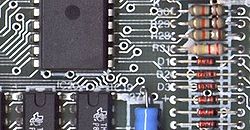
Plated-through holes on a multilayer board (magnified)
Double layered plating in CAD. Vias makes EDA placement possible. Bottom layer – Red Top layer – Blue
Plating of plated-through holes: Above – Top layer Down – Bottom layer
↑Through-holes per core. It is possible, though more expensive, to create blind or buried vias by using additional cores and lamination steps. It is also possible to backdrill and remove the plating from one side through to the desired layer, which leaves the physical hole as a through-hole, but creates the electrical equivalent of a blind via. If a PCB needs enough layers to justify blind and buried vias, it is probably also using small enough traces packed tightly enough to require (laser-drilled) microvias.
↑Gautam, Deepak; Wager, Dave; Musavi, Fariborz; Edington, Murray; Eberle, Wilson; Dunford, Willa G. (2013-03-17). A review of thermal management in power converters with thermal vias. 2013 Twenty-Eighth Annual IEEE Applied Power Electronics Conference and Exposition (APEC). Long Beach, California, U.S.A: IEEE. doi:10.1109/APEC.2013.6520276.
Dingler, Klaus; Musewski, Markus (2009-03-18). "Pluggen / Plugging". FED-Wiki (in German). Berlin, Germany: Fachverband Elektronik-Design e.V. (FED). Archived from the original on 2017-12-18. Retrieved 2017-12-18.
Brooks, Douglas G.; Adam, Johannes (2017-02-09). PCB Trace and Via Temperatures: The Complete Analysis (2nded.). CreateSpace Independent Publishing Platform. ISBN978-1541213524.
This page is based on this Wikipedia article Text is available under the CC BY-SA 4.0 license; additional terms may apply. Images, videos and audio are available under their respective licenses.


 Plated-through holes on a multilayer board (magnified)
 Plating of plated-through holes: