This article needs additional citations for verification .(July 2017) |

This article needs additional citations for verification .(July 2017) |

Programmable logic devices, such as programmable array logic and complex programmable logic devices, typically have a macrocell on every output pin.
A macrocell array is an approach to the design and manufacture of ASICs. Essentially, it is a small step up from the otherwise similar gate array, but rather than being a prefabricated array of simple logic gates, the macrocell array is a prefabricated array of higher-level logic functions such as flip-flops, ALU functions, registers, and the like. These logic functions are simply placed at regular predefined positions and manufactured on a wafer, usually called master slice. Creation of a circuit with a specified function is accomplished by adding metal interconnects to the chips on the master slice late in the manufacturing process, allowing the function of the chip to be customised as desired.
Macrocell array master slices are usually prefabricated and stockpiled in large quantities regardless of customer orders. The fabrication according to the individual customer specifications may be finished in a shorter time compared with standard cell or full custom design. The macrocell array approach reduces the mask costs since fewer custom masks need to be produced. In addition manufacturing test tooling lead time and costs are reduced since the same test fixtures may be used for all macrocell array products manufactured on the same die size.
Drawbacks are somewhat low density and performance than other approaches to ASIC design. However this style is often a viable approach for low production volumes.
A standard cell library is sometimes called a "macrocell library". [1] [2]
Processor design is a subfield of computer engineering and electronics engineering (fabrication) that deals with creating a processor, a key component of computer hardware.
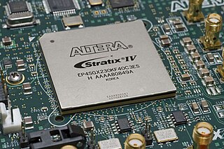
A field-programmable gate array (FPGA) is an integrated circuit designed to be configured by a customer or a designer after manufacturing – hence the term field-programmable. The FPGA configuration is generally specified using a hardware description language (HDL), similar to that used for an application-specific integrated circuit (ASIC). Circuit diagrams were previously used to specify the configuration, but this is increasingly rare due to the advent of electronic design automation tools.

An integrated circuit or monolithic integrated circuit is a set of electronic circuits on one small flat piece of semiconductor material, usually silicon. Large numbers of miniaturized transistors and other electronic components are integrated together on the chip. This results in circuits that are orders of magnitude smaller, faster, and less expensive than those constructed of discrete components, allowing a large transistor count. The IC's mass production capability, reliability, and building-block approach to integrated circuit design has ensured the rapid adoption of standardized ICs in place of designs using discrete transistors. ICs are now used in virtually all electronic equipment and have revolutionized the world of electronics. Computers, mobile phones and other home appliances are now inextricable parts of the structure of modern societies, made possible by the small size and low cost of ICs such as modern computer processors and microcontrollers.
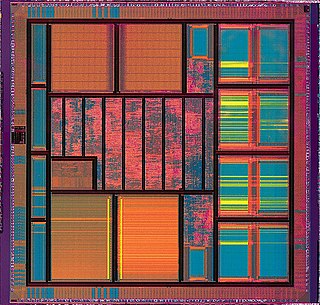
Very large-scale integration (VLSI) is the process of creating an integrated circuit (IC) by combining millions or billions of MOS transistors onto a single chip. VLSI began in the 1970s when MOS integrated circuit chips were developed and then widely adopted, enabling complex semiconductor and telecommunication technologies. The microprocessor and memory chips are VLSI devices.

A programmable logic device (PLD) is an electronic component used to build reconfigurable digital circuits. Unlike digital logic constructed using discrete logic gates with fixed functions, a PLD has an undefined function at the time of manufacture. Before the PLD can be used in a circuit it must be programmed to implement the desired function. Compared to fixed logic devices, programmable logic devices simplify the design of complex logic and may offer superior performance. Unlike for microprocessors, programming a PLD changes the connections made between the gates in the device.
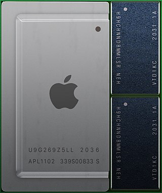
A system on a chip or system-on-chip is an integrated circuit that integrates most or all components of a computer or other electronic system. These components almost always include a central processing unit (CPU), memory interfaces, on-chip input/output devices, input/output interfaces, and secondary storage interfaces, often alongside other components such as radio modems and a graphics processing unit (GPU) – all on a single substrate or microchip. It may contain digital, and also analog, mixed-signal, and often radio frequency signal processing functions.

An application-specific integrated circuit is an integrated circuit (IC) chip customized for a particular use, rather than intended for general-purpose use, such as a chip designed to run in a digital voice recorder or a high-efficiency video codec. Application-specific standard product chips are intermediate between ASICs and industry standard integrated circuits like the 7400 series or the 4000 series. ASIC chips are typically fabricated using metal–oxide–semiconductor (MOS) technology, as MOS integrated circuit chips.
Electronic design automation (EDA), also referred to as electronic computer-aided design (ECAD), is a category of software tools for designing electronic systems such as integrated circuits and printed circuit boards. The tools work together in a design flow that chip designers use to design and analyze entire semiconductor chips. Since a modern semiconductor chip can have billions of components, EDA tools are essential for their design; this article in particular describes EDA specifically with respect to integrated circuits (ICs).

Altera Corporation was a manufacturer of programmable logic devices (PLDs) headquartered in San Jose, California. It was founded in 1983 and acquired by Intel in 2015.

Programmable Array Logic (PAL) is a family of programmable logic device semiconductors used to implement logic functions in digital circuits introduced by Monolithic Memories, Inc. (MMI) in March 1978. MMI obtained a registered trademark on the term PAL for use in "Programmable Semiconductor Logic Circuits". The trademark is currently held by Lattice Semiconductor.
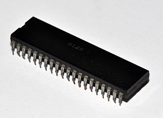
A gate array is an approach to the design and manufacture of application-specific integrated circuits (ASICs) using a prefabricated chip with components that are later interconnected into logic devices according to a custom order by adding metal interconnect layers in the factory. It was popular during upheaval in semiconductor industry in 80s and its usage declined by end of 90s.

A complex programmable logic device (CPLD) is a programmable logic device with complexity between that of PALs and FPGAs, and architectural features of both. The main building block of the CPLD is a macrocell, which contains logic implementing disjunctive normal form expressions and more specialized logic operations.
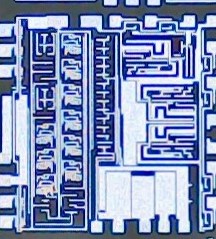
A mixed-signal integrated circuit is any integrated circuit that has both analog circuits and digital circuits on a single semiconductor die. Their usage has grown dramatically with the increased use of cell phones, telecommunications, portable electronics, and automobiles with electronics and digital sensors.
In electronic design, a semiconductor intellectual property core, IP core, or IP block is a reusable unit of logic, cell, or integrated circuit layout design that is the intellectual property of one party. IP cores can be licensed to another party or owned and used by a single party. The term comes from the licensing of the patent or source code copyright that exists in the design. Designers of application-specific integrated circuits (ASIC) and systems of field-programmable gate array (FPGA) logic can use IP cores as building blocks.
In semiconductor design, standard-cell methodology is a method of designing application-specific integrated circuits (ASICs) with mostly digital-logic features. Standard-cell methodology is an example of design abstraction, whereby a low-level very-large-scale integration (VLSI) layout is encapsulated into an abstract logic representation.

Hardware acceleration is the use of computer hardware designed to perform specific functions more efficiently when compared to software running on a general-purpose central processing unit (CPU). Any transformation of data that can be calculated in software running on a generic CPU can also be calculated in custom-made hardware, or in some mix of both.
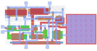
Integrated circuit design, or IC design, is a sub-field of electronics engineering, encompassing the particular logic and circuit design techniques required to design integrated circuits, or ICs. ICs consist of miniaturized electronic components built into an electrical network on a monolithic semiconductor substrate by photolithography.
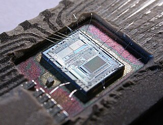
An electronic circuit is composed of individual electronic components, such as resistors, transistors, capacitors, inductors and diodes, connected by conductive wires or traces through which electric current can flow. It is a type of electrical circuit and to be referred to as electronic, rather than electrical, generally at least one active component must be present. The combination of components and wires allows various simple and complex operations to be performed: signals can be amplified, computations can be performed, and data can be moved from one place to another.

In integrated circuit design, physical design is a step in the standard design cycle which follows after the circuit design. At this step, circuit representations of the components of the design are converted into geometric representations of shapes which, when manufactured in the corresponding layers of materials, will ensure the required functioning of the components. This geometric representation is called integrated circuit layout. This step is usually split into several sub-steps, which include both design and verification and validation of the layout.
Field-programmable gate array prototyping, also referred to as FPGA-based prototyping, ASIC prototyping or system-on-chip (SoC) prototyping, is the method to prototype system-on-chip and application-specific integrated circuit designs on FPGAs for hardware verification and early software development.