Processor design is a subfield of computer engineering and electronics engineering (fabrication) that deals with creating a processor, a key component of computer hardware.

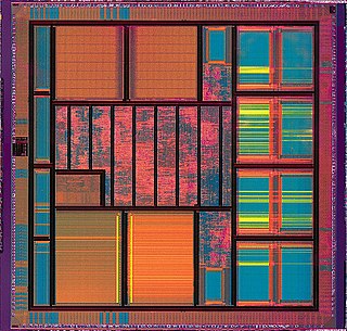
Very large-scale integration (VLSI) is the process of creating an integrated circuit (IC) by combining millions of MOS transistors onto a single chip. VLSI began in the 1970s when MOS integrated circuit chips were widely adopted, enabling complex semiconductor and telecommunication technologies to be developed. The microprocessor and memory chips are VLSI devices. Before the introduction of VLSI technology, most ICs had a limited set of functions they could perform. An electronic circuit might consist of a CPU, ROM, RAM and other glue logic. VLSI enables IC designers to add all of these into one chip.

A system on a chip is an integrated circuit that integrates all or most components of a computer or other electronic system. These components almost always include a central processing unit (CPU), memory, input/output ports and secondary storage, often alongside other components such as radio modems and a graphics processing unit (GPU) – all on a single substrate or microchip. It may contain digital, analog, mixed-signal, and often radio frequency signal processing functions.

An application-specific integrated circuit is an integrated circuit (IC) chip customized for a particular use, rather than intended for general-purpose use. For example, a chip designed to run in a digital voice recorder or a high-efficiency video codec is an ASIC. Application-specific standard product (ASSP) chips are intermediate between ASICs and industry standard integrated circuits like the 7400 series or the 4000 series. ASIC chips are typically fabricated using metal-oxide-semiconductor (MOS) technology, as MOS integrated circuit chips.
Electronic design automation (EDA), also referred to as electronic computer-aided design (ECAD), is a category of software tools for designing electronic systems such as integrated circuits and printed circuit boards. The tools work together in a design flow that chip designers use to design and analyze entire semiconductor chips. Since a modern semiconductor chip can have billions of components, EDA tools are essential for their design; this article in particular describes EDA specifically with respect to integrated circuits (ICs).

Altera Corporation was a manufacturer of programmable logic devices (PLDs) headquartered in San Jose, California. It was founded in 1983 and acquired by Intel in 2015.

A gate array is an approach to the design and manufacture of application-specific integrated circuits (ASICs) using a prefabricated chip with components that are later interconnected into logic devices according to a custom order by adding metal interconnect layers in the factory. It was popular during upheaval in semiconductor industry in 80s and its usage declined by end of 90s.

A mixed-signal integrated circuit is any integrated circuit that has both analog circuits and digital circuits on a single semiconductor die.
Semiconductor memory is a digital electronic semiconductor device used for digital data storage, such as computer memory. It typically refers to MOS memory, where data is stored within metal–oxide–semiconductor (MOS) memory cells on a silicon integrated circuit memory chip. There are numerous different types using different semiconductor technologies. The two main types of random-access memory (RAM) are static RAM (SRAM), which uses several MOS transistors per memory cell, and dynamic RAM (DRAM), which uses a MOS transistor and a MOS capacitor per cell. Non-volatile memory uses floating-gate memory cells, which consist of a single floating-gate MOS transistor per cell.
VLSI Technology, Inc., was an American company that designed and manufactured custom and semi-custom integrated circuits (ICs). The company was based in Silicon Valley, with headquarters at 1109 McKay Drive in San Jose. Along with LSI Logic, VLSI Technology defined the leading edge of the application-specific integrated circuit (ASIC) business, which accelerated the push of powerful embedded systems into affordable products.
In electronic design, a semiconductor intellectual property core, IP core, or IP block is a reusable unit of logic, cell, or integrated circuit layout design that is the intellectual property of one party. IP cores can be licensed to another party or owned and used by a single party. The term comes from the licensing of the patent or source code copyright that exists in the design. Designers of application-specific integrated circuits (ASIC) and systems of field-programmable gate array (FPGA) logic can use IP cores as building blocks.

In semiconductor design, standard cell methodology is a method of designing application-specific integrated circuits (ASICs) with mostly digital-logic features. Standard cell methodology is an example of design abstraction, whereby a low-level very-large-scale integration (VLSI) layout is encapsulated into an abstract logic representation.

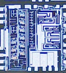
Integrated circuit design, or IC design, is a sub-field of electronics engineering, encompassing the particular logic and circuit design techniques required to design integrated circuits, or ICs. ICs consist of miniaturized electronic components built into an electrical network on a monolithic semiconductor substrate by photolithography.

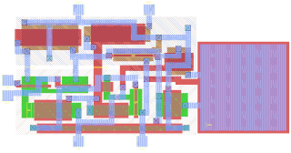
In integrated circuit design, physical design is a step in the standard design cycle which follows after the circuit design. At this step, circuit representations of the components of the design are converted into geometric representations of shapes which, when manufactured in the corresponding layers of materials, will ensure the required functioning of the components. This geometric representation is called integrated circuit layout. This step is usually split into several sub-steps, which include both design and verification and validation of the layout.
Structured ASIC is an intermediate technology between ASIC and FPGA, offering high performance, a characteristic of ASIC, and low NRE cost, a characteristic of FPGA. Using Structured ASIC allows products to be introduced quickly to market, to have lower cost and to be designed with ease.

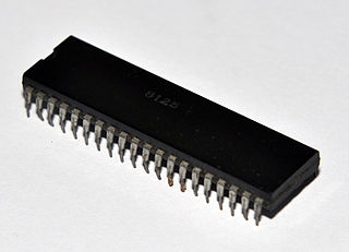
Read-only memory (ROM) is a type of non-volatile memory used in computers and other electronic devices. Data stored in ROM cannot be electronically modified after the manufacture of the memory device. Read-only memory is useful for storing software that is rarely changed during the life of the system, also known as firmware. Software applications for programmable devices can be distributed as plug-in cartridges containing ROM.

The VAX 6000 is a discontinued family of minicomputers developed and manufactured by Digital Equipment Corporation (DEC) using processors implementing the VAX instruction set architecture (ISA). Originally, the VAX 6000 was intended to be a mid-range VAX product line complementing the VAX 8000, but with the introduction of the VAX 6000 Model 400 series, the older VAX 8000 was discontinued in favor of the VAX 6000, which offered slightly higher performance for half the cost. The VAX 6000 family supports Digital's VMS and ULTRIX operating systems.
Power gating is a technique used in integrated circuit design to reduce power consumption, by shutting off the current to blocks of the circuit that are not in use. In addition to reducing stand-by or leakage power, power gating has the benefit of enabling Iddq testing.
NanGate, Inc was a privately held US/Silicon Valley-based multinational corporation dealing in Electronic Design Automation (EDA) for electrical engineering and electronics until its acquisition by Silvaco, Inc. in 2018. NanGate was founded in October 2004 by a group of semiconductor professionals with a background from Intel Corporation and Vitesse Semiconductor Corp. The company has received capital investments from a group of Danish business angels and venture capital companies. The company is today owned and controlled by its management following a management buy-out in 2012. NanGate markets a range of software products and design services for the design and optimization of standard cell libraries and application-specific integrated circuits. The market focus is standard cell library design and optimization for 14-28 nanometer CMOS processes.
