
An integrated circuit (IC), also known as a microchip, computer chip, or simply chip, is a small electronic device made up of multiple interconnected electronic components such as transistors, resistors, and capacitors. These components are etched onto a small piece of semiconductor material, usually silicon. Integrated circuits are used in a wide range of electronic devices, including computers, smartphones, and televisions, to perform various functions such as processing and storing information. They have greatly impacted the field of electronics by enabling device miniaturization and enhanced functionality.

An application-specific integrated circuit is an integrated circuit (IC) chip customized for a particular use, rather than intended for general-purpose use, such as a chip designed to run in a digital voice recorder or a high-efficiency video codec. Application-specific standard product chips are intermediate between ASICs and industry standard integrated circuits like the 7400 series or the 4000 series. ASIC chips are typically fabricated using metal–oxide–semiconductor (MOS) technology, as MOS integrated circuit chips.
Electronic design automation (EDA), also referred to as electronic computer-aided design (ECAD), is a category of software tools for designing electronic systems such as integrated circuits and printed circuit boards. The tools work together in a design flow that chip designers use to design and analyze entire semiconductor chips. Since a modern semiconductor chip can have billions of components, EDA tools are essential for their design; this article in particular describes EDA specifically with respect to integrated circuits (ICs).
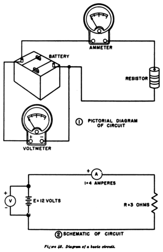
A circuit diagram is a graphical representation of an electrical circuit. A pictorial circuit diagram uses simple images of components, while a schematic diagram shows the components and interconnections of the circuit using standardized symbolic representations. The presentation of the interconnections between circuit components in the schematic diagram does not necessarily correspond to the physical arrangements in the finished device.

In integrated circuit design, integrated circuit (IC) layout, also known IC mask layout or mask design, is the representation of an integrated circuit in terms of planar geometric shapes which correspond to the patterns of metal, oxide, or semiconductor layers that make up the components of the integrated circuit. Originally the overall process was called tapeout, as historically early ICs used graphical black crepe tape on mylar media for photo imaging.
Schematic capture or schematic entry is a step in the design cycle of electronic design automation (EDA) at which the electronic diagram, or electronic schematic of the designed electronic circuit, is created by a designer. This is done interactively with the help of a schematic capture tool also known as schematic editor.
Place and route is a stage in the design of printed circuit boards, integrated circuits, and field-programmable gate arrays. As implied by the name, it is composed of two steps, placement and routing. The first step, placement, involves deciding where to place all electronic components, circuitry, and logic elements in a generally limited amount of space. This is followed by routing, which decides the exact design of all the wires needed to connect the placed components. This step must implement all the desired connections while following the rules and limitations of the manufacturing process.
In electronic design automation, a design rule is a geometric constraint imposed on circuit board, semiconductor device, and integrated circuit (IC) designers to ensure their designs function properly, reliably, and can be produced with acceptable yield. Design rules for production are developed by process engineers based on the capability of their processes to realize design intent. Electronic design automation is used extensively to ensure that designers do not violate design rules; a process called design rule checking (DRC). DRC is a major step during physical verification signoff on the design, which also involves LVS checks, XOR checks, ERC, and antenna checks. The importance of design rules and DRC is greatest for ICs, which have micro- or nano-scale geometries; for advanced processes, some fabs also insist upon the use of more restricted rules to improve yield.
VLSI Technology, Inc., was an American company that designed and manufactured custom and semi-custom integrated circuits (ICs). The company was based in Silicon Valley, with headquarters at 1109 McKay Drive in San Jose. Along with LSI Logic, VLSI Technology defined the leading edge of the application-specific integrated circuit (ASIC) business, which accelerated the push of powerful embedded systems into affordable products.

In semiconductor design, standard-cell methodology is a method of designing application-specific integrated circuits (ASICs) with mostly digital-logic features. Standard-cell methodology is an example of design abstraction, whereby a low-level very-large-scale integration (VLSI) layout is encapsulated into an abstract logic representation.

OrCAD Systems Corporation was a software company that made OrCAD, a proprietary software tool suite used primarily for electronic design automation (EDA). The software is used mainly by electronic design engineers and electronic technicians to create electronic schematics, and perform mixed-signal simulation and electronic prints for manufacturing printed circuit boards (PCBs). OrCAD was taken over by Cadence Design Systems in 1999 and was integrated with Cadence Allegro in 2005.
Integrated circuit design, semiconductor design, chip design or IC design, is a sub-field of electronics engineering, encompassing the particular logic and circuit design techniques required to design integrated circuits, or ICs. ICs consist of miniaturized electronic components built into an electrical network on a monolithic semiconductor substrate by photolithography.
Physical verification is a process whereby an integrated circuit layout design is verified via EDA software tools to ensure correct electrical and logical functionality and manufacturability. Verification involves design rule check (DRC), layout versus schematic (LVS), XOR, antenna checks and electrical rule check (ERC).

The Layout Versus Schematic (LVS) is the class of electronic design automation (EDA) verification software that determines whether a particular integrated circuit layout corresponds to the original schematic or circuit diagram of the design.

The Electric VLSI Design System is an EDA tool written in the early 1980s by Steven M. Rubin. Electric is used to construct logic wire schematics and to perform analysis of integrated circuit layout. It can also handle hardware description languages such as VHDL and Verilog. The system has many analysis and synthesis tools, including design rule checking, simulation, routing, Layout vs. Schematic, logical effort, and more.

In integrated circuit design, physical design is a step in the standard design cycle which follows after the circuit design. At this step, circuit representations of the components of the design are converted into geometric representations of shapes which, when manufactured in the corresponding layers of materials, will ensure the required functioning of the components. This geometric representation is called integrated circuit layout. This step is usually split into several sub-steps, which include both design and verification and validation of the layout.
In the automated design of integrated circuits, signoff checks is the collective name given to a series of verification steps that the design must pass before it can be taped out. This implies an iterative process involving incremental fixes across the board using one or more check types, and then retesting the design. There are two types of sign-off's: front-end sign-off and back-end sign-off. After back-end sign-off, the chip goes to fabrication. After listing out all the features in the specification, the verification engineer will write coverage for those features to identify bugs, and send back the RTL design to the designer. Bugs, or defects, can include issues like missing features, errors in design, etc. When the coverage reaches a maximum percentage then the verification team will sign it off. By using a methodology like UVM, OVM, or VMM, the verification team develops a reusable environment. Nowadays, UVM is more popular than others.
This page is a comparison of electronic design automation (EDA) software which is used today to design the near totality of electronic devices. Modern electronic devices are too complex to be designed without the help of a computer. Electronic devices may consist of integrated circuits (ICs), printed circuit boards (PCBs), field-programmable gate arrays (FPGAs) or a combination of them. Integrated circuits may consist of a combination of digital and analog circuits. These circuits can contain a combination of transistors, resistors, capacitors or specialized components such as analog neural networks, antennas or fuses.
In electronic design automation, parasitic extraction is the calculation of the parasitic effects in both the designed devices and the required wiring interconnects of an electronic circuit: parasitic capacitances, parasitic resistances and parasitic inductances, commonly called parasitic devices, parasitic components, or simply parasitics.

DesignSpark PCB is a free electronic design automation software package for printed circuit boards. Although there is no charge for the software, the user must register with DesignSpark.com to unlock the program and it displays advertisements which must be acknowledged before the user can begin working.