
The Layout Versus Schematic (LVS) is the class of electronic design automation (EDA) verification software that determines whether a particular integrated circuit layout corresponds to the original schematic or circuit diagram of the design.
The Layout Versus Schematic (LVS) is the class of electronic design automation (EDA) verification software that determines whether a particular integrated circuit layout corresponds to the original schematic or circuit diagram of the design.
A successful design rule check (DRC) ensures that the layout conforms to the rules designed/required for faultless fabrication. However, it does not guarantee if it really represents the circuit you desire to fabricate. This is where an LVS check is used.
The need for such programs was recognized relatively early in the history of ICs, and programs to perform this comparison were written as early as 1975. [1] These early programs operated mainly on the level of graph isomorphism, checking whether the schematic and layout were indeed identical. With the advent of digital logic, this was too restrictive, since exactly the same function can be implemented in many different (and non-isomorphic) ways. Therefore, LVS has been augmented by formal equivalence checking, which checks whether two circuits perform exactly the same function without demanding isomorphism. [2]
LVS checking software recognizes the drawn shapes of the layout that represent the electrical components of the circuit, as well as the connections between them. This netlist is compared by the "LVS" software against a similar schematic or circuit diagram's netlist.
LVS checking involves following three steps:
In most cases the layout will not pass LVS the first time requiring the layout engineer to examine the LVS software's reports and make changes to the layout. Typical errors encountered during LVS include:
Electronic design automation (EDA), also referred to as electronic computer-aided design (ECAD), is a category of software tools for designing electronic systems such as integrated circuits and printed circuit boards. The tools work together in a design flow that chip designers use to design and analyze entire semiconductor chips. Since a modern semiconductor chip can have billions of components, EDA tools are essential for their design; this article in particular describes EDA specifically with respect to integrated circuits (ICs).
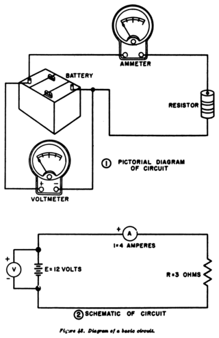
A circuit diagram is a graphical representation of an electrical circuit. A pictorial circuit diagram uses simple images of components, while a schematic diagram shows the components and interconnections of the circuit using standardized symbolic representations. The presentation of the interconnections between circuit components in the schematic diagram does not necessarily correspond to the physical arrangements in the finished device.
Silvaco Group, Inc., develops and markets electronic design automation (EDA) and technology CAD (TCAD) software and semiconductor design IP (SIP). The company is headquartered in Santa Clara, California, and has offices in North America, Europe, and throughout Asia. Founded in 1984, Silvaco is a publicly traded EDA company. The company has been known by at least two other names: Silvaco International, and Silvaco Data Systems.
Place and route is a stage in the design of printed circuit boards, integrated circuits, and field-programmable gate arrays. As implied by the name, it is composed of two steps, placement and routing. The first step, placement, involves deciding where to place all electronic components, circuitry, and logic elements in a generally limited amount of space. This is followed by routing, which decides the exact design of all the wires needed to connect the placed components. This step must implement all the desired connections while following the rules and limitations of the manufacturing process.
In electronic design automation, a design rule is a geometric constraint imposed on circuit board, semiconductor device, and integrated circuit (IC) designers to ensure their designs function properly, reliably, and can be produced with acceptable yield. Design rules for production are developed by process engineers based on the capability of their processes to realize design intent. Electronic design automation is used extensively to ensure that designers do not violate design rules; a process called design rule checking (DRC). DRC is a major step during physical verification signoff on the design, which also involves LVS checks, XOR checks, ERC, and antenna checks. The importance of design rules and DRC is greatest for ICs, which have micro- or nano-scale geometries; for advanced processes, some fabs also insist upon the use of more restricted rules to improve yield.

In semiconductor design, standard-cell methodology is a method of designing application-specific integrated circuits (ASICs) with mostly digital-logic features. Standard-cell methodology is an example of design abstraction, whereby a low-level very-large-scale integration (VLSI) layout is encapsulated into an abstract logic representation.

OrCAD Systems Corporation was a software company that made OrCAD, a proprietary software tool suite used primarily for electronic design automation (EDA). The software is used mainly by electronic design engineers and electronic technicians to create electronic schematics, and perform mixed-signal simulation and electronic prints for manufacturing printed circuit boards (PCBs). OrCAD was taken over by Cadence Design Systems in 1999 and was integrated with Cadence Allegro in 2005.

XCircuit is a schematic capture program for drawing publication-quality VLSI electrical circuit schematic diagrams and related figures. It's part of the Open Circuit Design tools. It's primarily intended for ULSI/VLSI IC design and not for PCB design, the latter though is still possible. XCircuit regards circuits as inherently hierarchical and can save circuits both in PostScript (.ps) and Ngspice (.cir) netlists file formats for further processing. The program compiles PostScript files from special template-labels specified by user.

Integrated circuit design, semiconductor design, chip design or IC design, is a sub-field of electronics engineering, encompassing the particular logic and circuit design techniques required to design integrated circuits, or ICs. ICs consist of miniaturized electronic components built into an electrical network on a monolithic semiconductor substrate by photolithography.
The electric circuit extraction or simply circuit extraction, also netlist extraction, is the translation of an integrated circuit layout back into the electrical circuit (netlist) it is intended to represent. This extracted circuit is needed for various purposes including circuit simulation, static timing analysis, signal integrity, power analysis and optimization, and logic to layout comparison. Each of these functions require a slightly different representation of the circuit, resulting in the need for multiple layout extractions. In addition, there may be a postprocessing step of converting the device-level circuit into a purely digital circuit, but this is not considered part of the extraction process.
Physical verification is a process whereby an integrated circuit layout design is verified via EDA software tools to ensure correct electrical and logical functionality and manufacturability. Verification involves design rule check (DRC), layout versus schematic (LVS), XOR, antenna checks and electrical rule check (ERC).
Quite Universal Circuit Simulator (Qucs) is a free-software electronics circuit simulator software application released under GPL. It offers the ability to set up a circuit with a graphical user interface and simulate the large-signal, small-signal and noise behaviour of the circuit. Pure digital simulations are also supported using VHDL and/or Verilog. Only a small set of digital devices like flip flops and logic gates can be used with analog circuits. Qucs uses its own SPICE-incompatible backend simulator Qucsator, however the Qucs-S fork supports some SPICE backends.

KiCad is a free software suite for electronic design automation (EDA). It facilitates the design and simulation of electronic hardware for PCB manufacturing. It features an integrated environment for schematic capture, PCB layout, manufacturing file viewing, ngspice-provided SPICE simulation, and engineering calculation. Tools exist within the package to create bill of materials, artwork, Gerber files, and 3D models of the PCB and its components.
An integrated circuit layout editor or IC layout editor is an electronic design automation software tool that allows a user to digitize the shapes and patterns that form an integrated circuit. Typically the view will include the components, metal routing tracks, vias and electrical pins. Software of this type is similar to computer aided drafting software, but is specialized for the task of integrated circuit layout. The typical flow for the layout of analog circuits might be :
This page is a comparison of electronic design automation (EDA) software which is used today to design the near totality of electronic devices. Modern electronic devices are too complex to be designed without the help of a computer. Electronic devices may consist of integrated circuits (ICs), printed circuit boards (PCBs), field-programmable gate arrays (FPGAs) or a combination of them. Integrated circuits may consist of a combination of digital and analog circuits. These circuits can contain a combination of transistors, resistors, capacitors or specialized components such as analog neural networks, antennas or fuses.
In electronic design automation, parasitic extraction is the calculation of the parasitic effects in both the designed devices and the required wiring interconnects of an electronic circuit: parasitic capacitances, parasitic resistances and parasitic inductances, commonly called parasitic devices, parasitic components, or simply parasitics.

PCB is a free and open-source software suite for electronic design automation (EDA) - for printed circuit boards (PCB) layout. It uses GTK+ for its GUI widgets.

DesignSpark PCB is a free electronic design automation software package for printed circuit boards. Although there is no charge for the software, the user must register with DesignSpark.com to unlock the program and it displays advertisements which must be acknowledged before the user can begin working.
LTspice is a SPICE-based analog electronic circuit simulator computer software, produced by semiconductor manufacturer Analog Devices. It is the most widely distributed and used SPICE software in the industry. Though it is freeware, LTspice is not artificially restricted to limit its capabilities. It ships with a library of SPICE models from Analog Devices, Linear Technology, Maxim Integrated, and third-party sources.

DipTrace is a proprietary software suite for electronic design automation (EDA) used for electronic schematic capture and printed circuit board layouts. DipTrace has four applications: schematic capture editor, PCB layout editor with built-in shape-based autorouter and 3D preview, component editor, and pattern editor.