
An operational amplifier is a DC-coupled high-gain electronic voltage amplifier with a differential input and, usually, a single-ended output. In this configuration, an op amp produces an output potential that is typically 100,000 times larger than the potential difference between its input terminals. The operational amplifier traces its origin and name to analog computers, where they were used to perform mathematical operations in linear, non-linear, and frequency-dependent circuits.
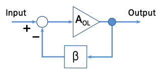
A negative-feedback amplifier is an electronic amplifier that subtracts a fraction of its output from its input, so that negative feedback opposes the original signal. The applied negative feedback can improve its performance and reduces sensitivity to parameter variations due to manufacturing or environment. Because of these advantages, many amplifiers and control systems use negative feedback.

In electronics, a common-base amplifier is one of three basic single-stage bipolar junction transistor (BJT) amplifier topologies, typically used as a current buffer or voltage amplifier.

A differential amplifier is a type of electronic amplifier that amplifies the difference between two input voltages but suppresses any voltage common to the two inputs. It is an analog circuit with two inputs and and one output , in which the output is ideally proportional to the difference between the two voltages:

A buffer amplifier is one that provides electrical impedance transformation from one circuit to another, with the aim of preventing the signal source from being affected by whatever currents that the load may impose. The signal is 'buffered from' load currents. Two main types of buffer exist: the voltage buffer and the current buffer.

In electronics, a common-emitter amplifier is one of three basic single-stage bipolar-junction-transistor (BJT) amplifier topologies, typically used as a voltage amplifier. It offers high current gain, medium input resistance and a high output resistance. The output of a common emitter amplifier is 180 degrees out of phase to the input signal.

In electronics, a common collector amplifier is one of three basic single-stage bipolar junction transistor (BJT) amplifier topologies, typically used as a voltage buffer.
Transconductance, also infrequently called mutual conductance, is the electrical characteristic relating the current through the output of a device to the voltage across the input of a device. Conductance is the reciprocal of resistance.

The output impedance of an electrical network is the measure of the opposition to current flow (impedance), both static (resistance) and dynamic (reactance), into the load network being connected that is internal to the electrical source. The output impedance is a measure of the source's propensity to drop in voltage when the load draws current, the source network being the portion of the network that transmits and the load network being the portion of the network that consumes.

A current source is an electronic circuit that delivers or absorbs an electric current which is independent of the voltage across it.

The asymptotic gain model is a representation of the gain of negative feedback amplifiers given by the asymptotic gain relation:
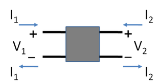
In electronics, a two-port network is an electrical network or device with two pairs of terminals to connect to external circuits. Two terminals constitute a port if the currents applied to them satisfy the essential requirement known as the port condition: the current entering one terminal must equal the current emerging from the other terminal on the same port. The ports constitute interfaces where the network connects to other networks, the points where signals are applied or outputs are taken. In a two-port network, often port 1 is considered the input port and port 2 is considered the output port.

In electronics, a common-source amplifier is one of three basic single-stage field-effect transistor (FET) amplifier topologies, typically used as a voltage or transconductance amplifier. The easiest way to tell if a FET is common source, common drain, or common gate is to examine where the signal enters and leaves. The remaining terminal is what is known as "common". In this example, the signal enters the gate, and exits the drain. The only terminal remaining is the source. This is a common-source FET circuit. The analogous bipolar junction transistor circuit may be viewed as a transconductance amplifier or as a voltage amplifier.. As a transconductance amplifier, the input voltage is seen as modulating the current going to the load. As a voltage amplifier, input voltage modulates the current flowing through the FET, changing the voltage across the output resistance according to Ohm's law. However, the FET device's output resistance typically is not high enough for a reasonable transconductance amplifier, nor low enough for a decent voltage amplifier. As seen below in the formula, the voltage gain depends on the load resistance, so it cannot be applied to drive low-resistance devices, such as a speaker. Another major drawback is the amplifier's limited high-frequency response. Therefore, in practice the output often is routed through either a voltage follower, or a current follower, to obtain more favorable output and frequency characteristics. The CS–CG combination is called a cascode amplifier.
In electronics, a common-drain amplifier, also known as a source follower, is one of three basic single-stage field-effect transistor (FET) amplifier topologies, typically used as a voltage buffer. In this circuit (NMOS) the gate terminal of the transistor serves as the signal input, the source is the output, and the drain is common to both, hence its name. Because of its low dependence on the load resistor on the voltage gain, it can be used to drive low resistance loads, such as a speaker. The analogous bipolar junction transistor circuit is the common-collector amplifier. This circuit is also commonly called a "stabilizer".
The cascode is a two-stage amplifier that consists of a common-emitter stage feeding into a common-base stage.
In electronics, the Miller effect accounts for the increase in the equivalent input capacitance of an inverting voltage amplifier due to amplification of the effect of capacitance between the input and output terminals. The virtually increased input capacitance due to the Miller effect is given by
A Wilson current mirror is a three-terminal circuit that accepts an input current at the input terminal and provides a "mirrored" current source or sink output at the output terminal. The mirrored current is a precise copy of the input current. It may be used as a Wilson current source by applying a constant bias current to the input branch as in Fig. 2. The circuit is named after George R. Wilson, an integrated circuit design engineer who worked for Tektronix. Wilson devised this configuration in 1967 when he and Barrie Gilbert challenged each other to find an improved current mirror overnight that would use only three transistors. Wilson won the challenge.

Distributed amplifiers are circuit designs that incorporate transmission line theory into traditional amplifier design to obtain a larger gain-bandwidth product than is realizable by conventional circuits.

The operational transconductance amplifier (OTA) is an amplifier whose differential input voltage produces an output current. Thus, it is a voltage controlled current source (VCCS). There is usually an additional input for a current to control the amplifier's transconductance. The OTA is similar to a standard operational amplifier in that it has a high impedance differential input stage and that it may be used with negative feedback.

An FET amplifier is an amplifier that uses one or more field-effect transistors (FETs). The most common type of FET amplifier is the MOSFET amplifier, which uses metal–oxide–semiconductor FETs (MOSFETs). The main advantage of a FET used for amplification is that it has very high input impedance and low output impedance.


