Small numbers of dopant atoms can change the ability of a semiconductor to conduct electricity. When on the order of one dopant atom is added per 100 million intrinsic atoms, the doping is said to be low or light. When many more dopant atoms are added, on the order of one per ten thousand atoms, the doping is referred to as high or heavy. This is often shown as n+ for n-type doping or p+ for p-type doping. (See the article on semiconductors for a more detailed description of the doping mechanism.) A semiconductor doped to such high levels that it acts more like a conductor than a semiconductor is referred to as a degenerate semiconductor. A semiconductor can be considered i-type semiconductor if it has been doped in equal quantities of p and n.
In the context of phosphors and scintillators, doping is better known as activation; this is not to be confused with dopant activation in semiconductors. Doping is also used to control the color in some pigments.
History
The effects of impurities in semiconductors (doping) were long known empirically in such devices as crystal radiodetectors and selenium rectifiers. For instance, in 1885 Shelford Bidwell, and in 1930 the German scientist Bernhard Gudden, each independently reported that the properties of semiconductors were due to the impurities they contained.[1][2] A doping process was formally developed by John Robert Woodyard working at Sperry Gyroscope Company during World War II. Though the word doping is not used in it, his US Patent issued in 1950 describes methods for adding tiny amounts of solid elements from the nitrogen column of the periodic table to germanium to produce rectifying devices.[3] The demands of his work on radar prevented Woodyard from pursuing further research on semiconductor doping.
Woodyard's prior patent proved to be the grounds of extensive litigation by Sperry Rand.[5]
Carrier concentration
The concentration of the dopant used affects many electrical properties of the semi-conductor. Most important is the material's charge carrier concentration. In an intrinsic semiconductor under thermal equilibrium, the concentrations of electrons and holes are equivalent. That is,
In a non-intrinsic semiconductor under thermal equilibrium, the relation becomes (for low doping):
where n0 is the concentration of conducting electrons, p0 is the conducting hole concentration, and ni is the material's intrinsic carrier concentration. The intrinsic carrier concentration varies between materials and is dependent on temperature. Silicon's ni, for example, is roughly 1.08×1010 cm−3 at 300 kelvins, about room temperature.[6]
In general, increased doping leads to increased conductivity due to the higher concentration of carriers. Degenerate (very highly doped) semiconductors have conductivity levels comparable to metals and are often used in integrated circuits as a replacement for metal. Often superscript plus and minus symbols are used to denote relative doping concentration in semiconductors. For example, n+ denotes an n-type semiconductor with a high, often degenerate, doping concentration. Similarly, p− would indicate a very lightly doped p-type material. Even degenerate levels of doping imply low concentrations of impurities with respect to the base semiconductor. In intrinsic crystalline silicon, there are approximately 5×10²² atoms/cm3. Doping concentration for silicon semiconductors may range anywhere from 1013 cm−3 to 1018 cm−3. Doping concentration above about 1018 cm−3 is considered degenerate at room temperature. Degenerately doped silicon contains a proportion of impurity to silicon on the order of parts per thousand. This proportion may be reduced to parts per billion in very lightly doped silicon. Typical concentration values fall somewhere in this range and are tailored to produce the desired properties in the device that the semiconductor is intended for.
Effect on band structure
Band diagram of PN junction operation in forward bias mode showing reducing depletion width. Both p and n junctions are doped at a 1×10 /cm doping level, leading to built-in potential of ~0.59 V. Reducing depletion width can be inferred from the shrinking charge profile, as fewer dopants are exposed with increasing forward bias.
Doping a semiconductor in a good crystal introduces allowed energy states within the band gap, but very close to the energy band that corresponds to the dopant type. In other words, electron donor impurities create states near the conduction band while electron acceptor impurities create states near the valence band. The gap between these energy states and the nearest energy band is usually referred to as dopant-site bonding energy or EB and is relatively small. For example, the EB for boron in silicon bulk is 0.045 eV, compared with silicon's band gap of about 1.12 eV. Because EB is so small, room temperature is hot enough to thermally ionize practically all of the dopant atoms and create free charge carriers in the conduction or valence bands.
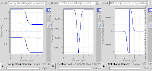
Dopants also have the important effect of shifting the energy bands relative to the Fermi level. The energy band that corresponds with the dopant with the greatest concentration ends up closer to the Fermi level. Since the Fermi level must remain constant in a system in thermodynamic equilibrium, stacking layers of materials with different properties leads to many useful electrical properties induced by band bending, if the interfaces can be made cleanly enough. For example, the p-n junction's properties are due to the band bending that happens as a result of the necessity to line up the bands in contacting regions of p-type and n-type material. This effect is shown in a band diagram. The band diagram typically indicates the variation in the valence band and conduction band edges versus some spatial dimension, often denoted x. The Fermi level is also usually indicated in the diagram. Sometimes the intrinsic Fermi level, Ei, which is the Fermi level in the absence of doping, is shown. These diagrams are useful in explaining the operation of many kinds of semiconductor devices.
Relationship to carrier concentration (low doping)
For low levels of doping, the relevant energy states are populated sparsely by electrons (conduction band) or holes (valence band). It is possible to write simple expressions for the electron and hole carrier concentrations, by ignoring Pauli exclusion (via Maxwell–Boltzmann statistics):
where EF is the Fermi level, EC is the minimum energy of the conduction band, and EV is the maximum energy of the valence band. These are related to the value of the intrinsic concentration via[7]
an expression which is independent of the doping level, since EC – EV (the band gap) does not change with doping.
The concentration factors NC(T) and NV(T) are given by
where me* and mh* are the density of states effective masses of electrons and holes, respectively, quantities that are roughly constant over temperature.[7]
Alternately, synthesis of semiconductor devices may involve the use of vapor-phase epitaxy. In vapor-phase epitaxy, a gas containing the dopant precursor can be introduced into the reactor. For example, in the case of n-type gas doping of gallium arsenide, hydrogen sulfide is added, and sulfur is incorporated into the structure.[9] This process is characterized by a constant concentration of sulfur on the surface.[10] In the case of semiconductors in general, only a very thin layer of the wafer needs to be doped in order to obtain the desired electronic properties.[11]
Post-growth doping
To define circuit elements, selected areas — typically controlled by photolithography[12] — are further doped by such processes as thermal diffusion doping (tube furnace diffusion) [13] and ion implantation, the latter method being more popular in large production runs for integrated circuits because of increased controllability.[14]
Thermal diffusion doping, simply known as diffusion, is widely used in silicon photovoltaics[15] and uses chemicals such as Boron tribromide or diborane[16] as a source for doping with boron.[17][18] With the diffusion process, the wafer is placed in a quartz tube furnace, using a quartz holder called a boat[19] at a temperature of 1200°C in which a chemical compound containing the dopant, such as Boron tribromide for doping with boron to create p-type semiconductor regions, or Phosphoryl chloride to create n-type regions,[20][21] is introduced into the furnace. This creates a layer of the dopant on the surface of the wafer and this step is called pre-deposition. Then a second step, called drive-in, is performed in which the wafer is heated at a higher temperature of 1300°C to introduce the dopant into the structure of the wafer.[22] Diffusion can use solid, liquid or gaseous sources with dopant atoms, such as solid boron nitride for boron, arsenic trioxide for arsenic, liquid arsenic trichloride, gaaseous arsine or phosphine. If using a gaseous source, it is carried to the furnace using a carrier gas such as nitrogen, and then allowed to decompose on the hot surface of the wafer, depositing the desired dopant, such as arsenic for example. If a liquid source is used, its vapors are carried to the furnace using nitrogen.[16][23][24] The furnace can be either horizontal or vertical.[25]
Spin-on glass
Spin-on glass or spin-on dopant doping is a two-step process. First, a mixture of SiO2 and dopants (in a solvent) is applied to a wafer surface by spin-coating. Then it is stripping and baked at a certain temperature in a furnace with constant nitrogen+oxygen flow.[26]
Neutrontransmutation doping (NTD) is an unusual doping method for special applications. Most commonly, it is used to dope silicon n-type in high-power electronics and semiconductor detectors. It is based on the conversion of the Si-30 isotope into phosphorus atom by neutron absorption as follows:
In practice, the silicon is typically placed near a nuclear reactor to receive the neutrons. As neutrons continue to pass through the silicon, more and more phosphorus atoms are produced by transmutation, and therefore the doping becomes more and more strongly n-type. NTD is a far less common doping method than diffusion or ion implantation, but it has the advantage of creating an extremely uniform dopant distribution.[27][28]
Dopant elements
Group IV semiconductors
(Note: When discussing periodic table groups, semiconductor physicists always use an older notation, not the current IUPAC group notation. For example, the carbon group is called "Group IV", not "Group 14".)
For the Group IV semiconductors such as diamond, silicon, germanium, silicon carbide, and silicon–germanium, the most common dopants are acceptors from Group III or donors from Group V elements. Boron, arsenic, phosphorus, and occasionally gallium are used to dope silicon. Boron is the p-type dopant of choice for silicon integrated circuit production because it diffuses at a rate that makes junction depths easily controllable. Phosphorus is typically used for bulk-doping of silicon wafers, while arsenic is used to diffuse junctions, because it diffuses more slowly than phosphorus and is thus more controllable.
By doping pure silicon with Group V elements such as phosphorus, extra valence electrons are added that become unbounded from individual atoms and allow the compound to be an electrically conductive n-type semiconductor. Doping with Group III elements, which are missing the fourth valence electron, creates "broken bonds" (holes) in the silicon lattice that are free to move. The result is an electrically conductive p-type semiconductor. In this context, a Group V element is said to behave as an electron donor, and a Group III element as an acceptor. This is a key concept in the physics of a diode.
A very heavily doped semiconductor behaves more like a good conductor (metal) and thus exhibits more linear positive thermal coefficient. Such effect is used for instance in sensistors.[29] Lower dosage of doping is used in other types (NTC or PTC) thermistors.
Silicon dopants
Acceptors, p-type
Boron is a p-type dopant. Its diffusion rate allows easy control of junction depths. Common in CMOS technology. Can be added by diffusion of diborane gas. The only acceptor with sufficient solubility for efficient emitters in transistors and other applications requiring extremely high dopant concentrations. Boron diffuses about as fast as phosphorus.
Aluminum, used for deep p-diffusions. Not popular in VLSI and ULSI. Also a common unintentional impurity.[30]
Gallium is a dopant used for long-wavelength infrared photoconduction silicon detectors in the 8–14 μm atmospheric window.[31] Gallium-doped silicon is also promising for solar cells, due to its long minority carrier lifetime with no lifetime degradation; as such it is gaining importance as a replacement of boron doped substrates for solar cell applications.[30]
Indium is a dopant used for long-wavelength infrared photoconduction silicon detectors in the 3–5 μm atmospheric window.[31]
Donors, n-type
Phosphorus is a n-type dopant. It diffuses fast, so is usually used for bulk doping, or for well formation. Used in solar cells. Can be added by diffusion of phosphine gas. Bulk doping can be achieved by nuclear transmutation, by irradiation of pure silicon with neutrons in a nuclear reactor. Phosphorus also traps gold atoms, which otherwise quickly diffuse through silicon and act as recombination centers.
Arsenic is a n-type dopant. Its slower diffusion allows using it for diffused junctions. Used for buried layers. Has similar atomic radius to silicon, high concentrations can be achieved. Its diffusivity is about a tenth of phosphorus or boron, so it is used where the dopant should stay in place during subsequent thermal processing. Useful for shallow diffusions where well-controlled abrupt boundary is desired. Preferred dopant in VLSI circuits. Preferred dopant in low resistivity ranges.[30]
Antimony is a n-type dopant. It has a small diffusion coefficient. Used for buried layers. Has diffusivity similar to arsenic, is used as its alternative. Its diffusion is virtually purely substitutional, with no interstitials, so it is free of anomalous effects. For this superior property, it is sometimes used in VLSI instead of arsenic. Heavy doping with antimony is important for power devices. Heavily antimony-doped silicon has lower concentration of oxygen impurities; minimal autodoping effects make it suitable for epitaxial substrates.[30]
Bismuth is a promising dopant for long-wavelength infrared photoconduction silicon detectors, a viable n-type alternative to the p-type gallium-doped material.[32]
Lithium is used for doping silicon for radiation hardened solar cells. The lithium presence anneals defects in the lattice produced by protons and neutrons.[33] Lithium can be introduced to boron-doped p+ silicon, in amounts low enough to maintain the p character of the material, or in large enough amount to counterdope it to low-resistivity n type.[34]
Other
Germanium can be used for band gap engineering. Germanium layer also inhibits diffusion of boron during the annealing steps, allowing ultrashallow p-MOSFET junctions.[35] Germanium bulk doping suppresses large void defects, increases internal gettering, and improves wafer mechanical strength.[30]
Silicon, germanium and xenon can be used as ion beams for pre-amorphization of silicon wafer surfaces. Formation of an amorphous layer beneath the surface allows forming ultrashallow junctions for p-MOSFETs.
Nitrogen is important for growing defect-free silicon crystal. Improves mechanical strength of the lattice, increases bulk microdefect generation, suppresses vacancy agglomeration.[30]
Gold and platinum are used for minority carrier lifetime control. They are used in some infrared detection applications. Gold introduces a donor level 0.35 eV above the valence band and an acceptor level 0.54 eV below the conduction band. Platinum introduces a donor level also at 0.35 eV above the valence band, but its acceptor level is only 0.26 eV below conduction band; as the acceptor level in n-type silicon is shallower, the space charge generation rate is lower and therefore the leakage current is also lower than for gold doping. At high injection levels platinum performs better for lifetime reduction. Reverse recovery of bipolar devices is more dependent on the low-level lifetime, and its reduction is better performed by gold. Gold provides a good tradeoff between forward voltage drop and reverse recovery time for fast switching bipolar devices, where charge stored in base and collector regions must be minimized. Conversely, in many power transistors a long minority carrier lifetime is required to achieve good gain, and the gold/platinum impurities must be kept low.[36]
Other semiconductors
In the following list the "(substituting X)" refers to all of the materials preceding said parenthesis.[37]
p-type: magnesium (substituting Ga) - challenging due to relatively high ionisation energy above the valence band edge, strong diffusion of interstitial Mg, hydrogen complexes passivating of Mg acceptors and by Mg self-compensation at higher concentrations)
In most cases many types of impurities will be present in the resultant doped semiconductor. If an equal number of donors and acceptors are present in the semiconductor, the extra core electrons provided by the former will be used to satisfy the broken bonds due to the latter, so that doping produces no free carriers of either type. This phenomenon is known as compensation, and occurs at the p-n junction in the vast majority of semiconductor devices.[citation needed]
Partial compensation, where donors outnumber acceptors or vice versa, allows device makers to repeatedly reverse (invert) the type of a certain layer under the surface of a bulk semiconductor by diffusing or implanting successively higher doses of dopants, so-called counterdoping. Most modern semiconductor devices are made by successive selective counterdoping steps to create the necessary P and N type areas under the surface of bulk silicon.[38] This is an alternative to successively growing such layers by epitaxy.
Although compensation can be used to increase or decrease the number of donors or acceptors, the electron and hole mobility is always decreased by compensation because mobility is affected by the sum of the donor and acceptor ions.[citation needed]
Conductive polymers can be doped by adding chemical reactants to oxidize, or sometimes reduce, the system so that electrons are pushed into the conducting orbitals within the already potentially conducting system. There are two primary methods of doping a conductive polymer, both of which use an oxidation-reduction (i.e., redox) process.
Chemical doping involves exposing a polymer such as melanin, typically a thin film, to an oxidant such as iodine or bromine. Alternatively, the polymer can be exposed to a reductant; this method is far less common, and typically involves alkali metals.
Electrochemical doping involves suspending a polymer-coated, working electrode in an electrolyte solution in which the polymer is insoluble along with separate counter and reference electrodes. An electric potential difference is created between the electrodes that causes a charge and the appropriate counter ion from the electrolyte to enter the polymer in the form of electron addition (i.e., n-doping) or removal (i.e., p-doping).
N-doping is much less common because the Earth's atmosphere is oxygen-rich, thus creating an oxidizing environment. An electron-rich, n-doped polymer will react immediately with elemental oxygen to de-dope (i.e., reoxidize to the neutral state) the polymer. Thus, chemical n-doping must be performed in an environment of inert gas (e.g., argon). Electrochemical n-doping is far more common in research, because it is easier to exclude oxygen from a solvent in a sealed flask. However, it is unlikely that n-doped conductive polymers are available commercially.[citation needed]
Doping in organic molecular semiconductors
Molecular dopants are preferred in doping molecular semiconductors due to their compatibilities of processing with the host, that is, similar evaporation temperatures or controllable solubility.[39] Additionally, the relatively large sizes of molecular dopants compared with those of metal ion dopants (such as Li+ and Mo6+) are generally beneficial, yielding excellent spatial confinement for use in multilayer structures, such as OLEDs and Organic solar cells. Typical p-type dopants include F4-TCNQ[40] and Mo(tfd)3.[41] However, similar to the problem encountered in doping conductive polymers, air-stable n-dopants suitable for materials with low electron affinity (EA) are still elusive. Recently, photoactivation with a combination of cleavable dimeric dopants, such as [RuCp∗Mes]2, suggests a new path to realize effective n-doping in low-EA materials.[39]
Research on magnetic doping has shown that considerable alteration of certain properties such as specific heat may be affected by small concentrations of an impurity; for example, dopant impurities in semiconducting ferromagnetic alloys can generate different properties as first predicted by White, Hogan, Suhl and Nakamura.[42][43] The inclusion of dopant elements to impart dilute magnetism is of growing significance in the field of magnetic semiconductors. The presence of disperse ferromagnetic species is key to the functionality of emerging spintronics, a class of systems that utilise electron spin in addition to charge. Using density functional theory (DFT) the temperature dependent magnetic behaviour of dopants within a given lattice can be modeled to identify candidate semiconductor systems.[44]
Single dopants in semiconductors
The sensitive dependence of a semiconductor's properties on dopants has provided an extensive range of tunable phenomena to explore and apply to devices. It is possible to identify the effects of a solitary dopant on commercial device performance as well as on the fundamental properties of a semiconductor material. New applications have become available that require the discrete character of a single dopant, such as single-spin devices in the area of quantum information or single-dopant transistors. Dramatic advances in the past decade towards observing, controllably creating and manipulating single dopants, as well as their application in novel devices have allowed opening the new field of solotronics (solitary dopant optoelectronics).[45]
Modulation doping
Electrons or holes introduced by doping are mobile, and can be spatially separated from dopant atoms they have dissociated from. Ionized donors and acceptors however attract electrons and holes, respectively, so this spatial separation requires abrupt changes of dopant levels, of band gap (e.g. a quantum well), or built-in electric fields (e.g. in case of noncentrosymmetric crystals). This technique is called modulation doping and is advantageous owing to suppressed carrier-donor scattering, allowing very high mobility to be attained.
↑ Sproul, A. B; Green, M. A (1991). "Improved value for the silicon intrinsic carrier concentration from 275 to 375 K". J. Appl. Phys. 70 (2): 846. Bibcode:1991JAP....70..846S. doi:10.1063/1.349645.
1 2 Green, M. A. (1990). "Intrinsic concentration, effective densities of states, and effective mass in silicon". Journal of Applied Physics. 67 (6): 2944. Bibcode:1990JAP....67.2944G. doi:10.1063/1.345414.
↑ Saga, Tatsuo (July 2010). "Advances in crystalline silicon solar cell technology for industrial mass production". NPG Asia Materials. 2 (3): 96–102. doi:10.1038/asiamat.2010.82.
↑ Lohmüller, E.; Glatz, M.; Lohmüller, S.; Belledin, U.; Mack, S.; Fellmeth, T.; Naber, R.C.G.; Wolf, A. (2020). BBr3 Diffusion: Process Optimization for High-Quality Emitters with Industrial Cycle Times. 37th European Photovoltaic Solar Energy Conference and Exhibition. pp.364–369. doi:10.4229/EUPVSEC20202020-2CV.1.43.
↑ Li, Mengjie; Ma, Fa-Jun; Peters, Ian Marius; Shetty, Kishan Devappa; Aberle, Armin G.; Hoex, Bram; Samudra, Ganesh S. (May 2017). "Numerical Simulation of Doping Process by BBr3 Tube Diffusion for Industrial n -Type Silicon Wafer Solar Cells". IEEE Journal of Photovoltaics. 7 (3): 755–762. doi:10.1109/JPHOTOV.2017.2679342.
↑ Cheng, Zhaoyang; Liu, Xiaozhen; Xie, Junyu; Zuo, Zhuliang (2024). "Diffusion and Ion Implantation Equipment". Handbook of Integrated Circuit Industry. pp.1361–1382. doi:10.1007/978-981-99-2836-1_66. ISBN978-981-99-2835-4.
↑ Park, Chan-Hyuck; Pan, Han; Ishikawa, Yasuhiko; Wada, Kazumi; Ahn, Donghwan (September 2018). "N-type doping of germanium epilayer on silicon by ex-situ phosphorus diffusion based on POCl3 phosphosilicate glass". Thin Solid Films. 662: 1–5. Bibcode:2018TSF...662....1P. doi:10.1016/j.tsf.2018.07.028.
↑ Li, Hongzhao; Kim, Kyung; Hallam, Brett; Hoex, Bram; Wenham, Stuart; Abbott, Malcolm (March 2017). "POCl3 diffusion for industrial Si solar cell emitter formation". Frontiers in Energy. 11 (1): 42–51. doi:10.1007/s11708-016-0433-7.
↑ Parry, Christopher M. (1981). "Bismuth-Doped Silicon: An Extrinsic Detector for Long-Wavelength Infrared (LWIR) Applications". In Chan, William S. (ed.). Mosaic Focal Plane Methodologies I. Vol.0244. pp.2–8. doi:10.1117/12.959299.
↑ Lin, Xin; Purdum, Geoffrey E.; Zhang, Yadong; Barlow, Stephen; Marder, Seth R.; Loo, Yueh-Lin; Kahn, Antoine (26 April 2016). "Impact of a Low Concentration of Dopants on the Distribution of Gap States in a Molecular Semiconductor". Chemistry of Materials. 28 (8): 2677–2684. doi:10.1021/acs.chemmater.6b00165.
This page is based on this Wikipedia article Text is available under the CC BY-SA 4.0 license; additional terms may apply. Images, videos and audio are available under their respective licenses.