Related Research Articles
A semiconductor is a material that has an electrical conductivity value falling between that of a conductor, such as copper, and an insulator, such as glass. Its resistivity generally falls as its temperature rises; metals behave in the opposite way. In many cases their conducting properties may be altered in useful ways by introducing impurities ("doping") into the crystal structure. When two differently doped regions exist in the same crystal, a semiconductor junction is created. The behavior of charge carriers, which include electrons, ions, and electron holes, at these junctions is the basis of diodes, transistors, and most modern electronics. Some examples of semiconductors are silicon, germanium, gallium arsenide, and elements near the so-called "metalloid staircase" on the periodic table. After silicon, gallium arsenide is the second-most common semiconductor and is used in laser diodes, solar cells, microwave-frequency integrated circuits, and others. Silicon is a critical element for fabricating most electronic circuits.

Solder is a fusible metal alloy used to create a permanent bond between metal workpieces. Solder is melted in order to wet the parts of the joint, where it adheres to and connects the pieces after cooling. Metals or alloys suitable for use as solder should have a lower melting point than the pieces to be joined. The solder should also be resistant to oxidative and corrosive effects that would degrade the joint over time. Solder used in making electrical connections also needs to have favorable electrical characteristics.
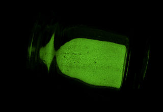
A phosphor is a substance that exhibits the phenomenon of luminescence; it emits light when exposed to some type of radiant energy. The term is used both for fluorescent or phosphorescent substances which glow on exposure to ultraviolet or visible light, and cathodoluminescent substances which glow when struck by an electron beam in a cathode-ray tube.

Gallium arsenide (GaAs) is a III-V direct band gap semiconductor with a zinc blende crystal structure.

Indium tin oxide (ITO) is a ternary composition of indium, tin and oxygen in varying proportions. Depending on the oxygen content, it can be described as either a ceramic or an alloy. Indium tin oxide is typically encountered as an oxygen-saturated composition with a formulation of 74% In, 8% Sn, and 18% O by weight. Oxygen-saturated compositions are so typical that unsaturated compositions are termed oxygen-deficient ITO. It is transparent and colorless in thin layers, while in bulk form it is yellowish to gray. In the infrared region of the spectrum it acts as a metal-like mirror.
In solid state physics, a charge carrier is a particle or quasiparticle that is free to move, carrying an electric charge, especially the particles that carry electric charges in electrical conductors. Examples are electrons, ions and holes. In a conducting medium, an electric field can exert force on these free particles, causing a net motion of the particles through the medium; this is what constitutes an electric current. The electron and the proton are the elementary charge carriers, each carrying one elementary charge (e), of the same magnitude and opposite sign.

A semimetal is a material with a small energy overlap between the bottom of the conduction band and the top of the valence band, but they do not overlap in momentum space. According to electronic band theory, solids can be classified as insulators, semiconductors, semimetals, or metals. In insulators and semiconductors the filled valence band is separated from an empty conduction band by a band gap. For insulators, the magnitude of the band gap is larger than that of a semiconductor. Because of the slight overlap between the conduction and valence bands, semimetals have no band gap and a small density of states at the Fermi level. A metal, by contrast, has an appreciable density of states at the Fermi level because the conduction band is partially filled.

A high-electron-mobility transistor, also known as heterostructure FET (HFET) or modulation-doped FET (MODFET), is a field-effect transistor incorporating a junction between two materials with different band gaps as the channel instead of a doped region. A commonly used material combination is GaAs with AlGaAs, though there is wide variation, dependent on the application of the device. Devices incorporating more indium generally show better high-frequency performance, while in recent years, gallium nitride HEMTs have attracted attention due to their high-power performance.

In semiconductor production, doping is the intentional introduction of impurities into an intrinsic (undoped) semiconductor for the purpose of modulating its electrical, optical and structural properties. The doped material is referred to as an extrinsic semiconductor.
Magnetic semiconductors are semiconductor materials that exhibit both ferromagnetism and useful semiconductor properties. If implemented in devices, these materials could provide a new type of control of conduction. Whereas traditional electronics are based on control of charge carriers, practical magnetic semiconductors would also allow control of quantum spin state. This would theoretically provide near-total spin polarization, which is an important property for spintronics applications, e.g. spin transistors.
An ohmic contact is a non-rectifying electrical junction: a junction between two conductors that has a linear current–voltage (I–V) curve as with Ohm's law. Low-resistance ohmic contacts are used to allow charge to flow easily in both directions between the two conductors, without blocking due to rectification or excess power dissipation due to voltage thresholds.
Capacitance–voltage profiling is a technique for characterizing semiconductor materials and devices. The applied voltage is varied, and the capacitance is measured and plotted as a function of voltage. The technique uses a metal–semiconductor junction or a p–n junction or a MOSFET to create a depletion region, a region which is empty of conducting electrons and holes, but may contain ionized donors and electrically active defects or traps. The depletion region with its ionized charges inside behaves like a capacitor. By varying the voltage applied to the junction it is possible to vary the depletion width. The dependence of the depletion width upon the applied voltage provides information on the semiconductor's internal characteristics, such as its doping profile and electrically active defect densities., Measurements may be done at DC, or using both DC and a small-signal AC signal, or using a large-signal transient voltage.

Indium(III) oxide (In2O3) is a chemical compound, an amphoteric oxide of indium.
Hot carrier injection (HCI) is a phenomenon in solid-state electronic devices where an electron or a “hole” gains sufficient kinetic energy to overcome a potential barrier necessary to break an interface state. The term "hot" refers to the effective temperature used to model carrier density, not to the overall temperature of the device. Since the charge carriers can become trapped in the gate dielectric of a MOS transistor, the switching characteristics of the transistor can be permanently changed. Hot-carrier injection is one of the mechanisms that adversely affects the reliability of semiconductors of solid-state devices.
An extrinsic semiconductor is one that has been doped; during manufacture of the semiconductor crystal a trace element or chemical called a doping agent has been incorporated chemically into the crystal, for the purpose of giving it different electrical properties than the pure semiconductor crystal, which is called an intrinsic semiconductor. In an extrinsic semiconductor it is these foreign dopant atoms in the crystal lattice that mainly provide the charge carriers which carry electric current through the crystal. The doping agents used are of two types, resulting in two types of extrinsic semiconductor. An electron donor dopant is an atom which, when incorporated in the crystal, releases a mobile conduction electron into the crystal lattice. An extrinsic semiconductor that has been doped with electron donor atoms is called an n-type semiconductor, because the majority of charge carriers in the crystal are negative electrons. An electron acceptor dopant is an atom which accepts an electron from the lattice, creating a vacancy where an electron should be called a hole which can move through the crystal like a positively charged particle. An extrinsic semiconductor which has been doped with electron acceptor atoms is called a p-type semiconductor, because the majority of charge carriers in the crystal are positive holes.

In semiconductor physics, an acceptor is a dopant atom that when substituted into a semiconductor lattice forms a p-type region.

Transparent conducting films (TCFs) are thin films of optically transparent and electrically conductive material. They are an important component in a number of electronic devices including liquid-crystal displays, OLEDs, touchscreens and photovoltaics. While indium tin oxide (ITO) is the most widely used, alternatives include wider-spectrum transparent conductive oxides (TCOs), conductive polymers, metal grids and random metallic networks, carbon nanotubes (CNT), graphene, nanowire meshes and ultra thin metal films.
A dopant is a small amount of a substance added to a material to alter its physical properties, such as electrical or optical properties. The amount of dopant is typically very low compared to the material being doped.
Band-gap engineering is the process of controlling or altering the band gap of a material. This is typically done to semiconductors by controlling the composition of alloys, constructing layered materials with alternating compositions, or by inducing strain either epitaxially or topologically. A band gap is the range in a solid where no electron state can exist. The band gap of insulators is much larger than in semiconductors. Conductors or metals have a much smaller or nonexistent band gap than semiconductors since the valence and conduction bands overlap. Controlling the band gap allows for the creation of desirable electrical properties.
References
- ↑ Hidenori Hiramatsu; Kazushige Ueda; Hiromichi Ohta; Masahiro Hirano; Toshio Kamiya; Hideo Hosono (15 December 2003). Wide gap p-type degenerate semiconductor: Mg-doped LaCuOSe. Thin Solid Films, Proceedings of the 3rd International Symposium on Transparent Oxide Thin films for Electronics and Optics. Vol. 445. pp. 304–308.
- ↑ Scott H. Brewer; Stefan Franzen (2002). "Indium Tin Oxide Plasma Frequency Dependence on Sheet Resistance and Surface Adlayers Determined by Reflectance FTIR Spectroscopy". J. Phys. Chem. B. 106 (50): 12986–12992. doi:10.1021/jp026600x.