A semiconductor is a material which has an electrical conductivity value falling between that of a conductor, such as copper, and an insulator, such as glass. Its resistivity falls as its temperature rises; metals behave in the opposite way. Its conducting properties may be altered in useful ways by introducing impurities ("doping") into the crystal structure. When two differently doped regions exist in the same crystal, a semiconductor junction is created. The behavior of charge carriers, which include electrons, ions, and electron holes, at these junctions is the basis of diodes, transistors, and most modern electronics. Some examples of semiconductors are silicon, germanium, gallium arsenide, and elements near the so-called "metalloid staircase" on the periodic table. After silicon, gallium arsenide is the second-most common semiconductor and is used in laser diodes, solar cells, microwave-frequency integrated circuits, and others. Silicon is a critical element for fabricating most electronic circuits.
Electrical resistivity is a fundamental property of a material that measures how strongly it resists electric current. A low resistivity indicates a material that readily allows electric current. Resistivity is commonly represented by the Greek letter ρ (rho). The SI unit of electrical resistivity is the ohm-meter (Ω⋅m). For example, if a 1 m3 solid cube of material has sheet contacts on two opposite faces, and the resistance between these contacts is 1 Ω, then the resistivity of the material is 1 Ω⋅m.
In solid state physics, a particle's effective mass is the mass that it seems to have when responding to forces, or the mass that it seems to have when interacting with other identical particles in a thermal distribution. One of the results from the band theory of solids is that the movement of particles in a periodic potential, over long distances larger than the lattice spacing, can be very different from their motion in a vacuum. The effective mass is a quantity that is used to simplify band structures by modeling the behavior of a free particle with that mass. For some purposes and some materials, the effective mass can be considered to be a simple constant of a material. In general, however, the value of effective mass depends on the purpose for which it is used, and can vary depending on a number of factors.
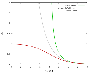
Fermi–Dirac statistics is a type of quantum statistics that applies to the physics of a system consisting of many non-interacting, identical particles that obey the Pauli exclusion principle. A result is the Fermi–Dirac distribution of particles over energy states. It is named after Enrico Fermi and Paul Dirac, each of whom derived the distribution independently in 1926. Fermi–Dirac statistics is a part of the field of statistical mechanics and uses the principles of quantum mechanics.
Space charge is an interpretation of a collection of electric charges in which excess electric charge is treated as a continuum of charge distributed over a region of space rather than distinct point-like charges. This model typically applies when charge carriers have been emitted from some region of a solid—the cloud of emitted carriers can form a space charge region if they are sufficiently spread out, or the charged atoms or molecules left behind in the solid can form a space charge region.

A p–n junction is a boundary or interface between two types of semiconductor materials, p-type and n-type, inside a single crystal of semiconductor. The "p" (positive) side contains an excess of holes, while the "n" (negative) side contains an excess of electrons in the outer shells of the electrically neutral atoms there. This allows electrical current to pass through the junction only in one direction. The p-n junction is created by doping, for example by ion implantation, diffusion of dopants, or by epitaxy. If two separate pieces of material were used, this would introduce a grain boundary between the semiconductors that would severely inhibit its utility by scattering the electrons and holes.
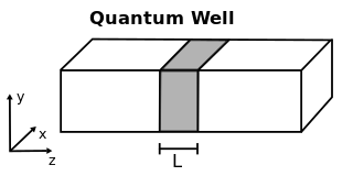
A quantum well is a potential well with only discrete energy values.
A heterojunction is an interface between two layers or regions of dissimilar semiconductors. These semiconducting materials have unequal band gaps as opposed to a homojunction. It is often advantageous to engineer the electronic energy bands in many solid-state device applications, including semiconductor lasers, solar cells and transistors. The combination of multiple heterojunctions together in a device is called a heterostructure, although the two terms are commonly used interchangeably. The requirement that each material be a semiconductor with unequal band gaps is somewhat loose, especially on small length scales, where electronic properties depend on spatial properties. A more modern definition of heterojunction is the interface between any two solid-state materials, including crystalline and amorphous structures of metallic, insulating, fast ion conductor and semiconducting materials.
In solid-state physics, the electron mobility characterises how quickly an electron can move through a metal or semiconductor when pulled by an electric field. There is an analogous quantity for holes, called hole mobility. The term carrier mobility refers in general to both electron and hole mobility.
In semiconductor production, doping is the intentional introduction of impurities into an intrinsic semiconductor for the purpose of modulating its electrical, optical and structural properties. The doped material is referred to as an extrinsic semiconductor.
In semiconductor physics, the depletion region, also called depletion layer, depletion zone, junction region, space charge region or space charge layer, is an insulating region within a conductive, doped semiconductor material where the mobile charge carriers have been diffused away, or have been forced away by an electric field. The only elements left in the depletion region are ionized donor or acceptor impurities.
In the solid-state physics of semiconductors, carrier generation and carrier recombination are processes by which mobile charge carriers are created and eliminated. Carrier generation and recombination processes are fundamental to the operation of many optoelectronic semiconductor devices, such as photodiodes, light-emitting diodes and laser diodes. They are also critical to a full analysis of p-n junction devices such as bipolar junction transistors and p-n junction diodes.
Charge carrier density, also known as carrier concentration, denotes the number of charge carriers in per volume. In SI units, it is measured in m−3. As with any density, in principle it can depend on position. However, usually carrier concentration is given as a single number, and represents the average carrier density over the whole material.
In solid-state physics, the Poole–Frenkel effect is a model describing the mechanism of trap-assisted electron transport in an electrical insulator. It is named after Yakov Frenkel, who published on it in 1938, extending the theory previously developed by H. H. Poole.

In semiconductor physics, the band gap of a semiconductor can be of two basic types, a direct band gap or an indirect band gap. The minimal-energy state in the conduction band and the maximal-energy state in the valence band are each characterized by a certain crystal momentum (k-vector) in the Brillouin zone. If the k-vectors are different, the material has an "indirect gap". The band gap is called "direct" if the crystal momentum of electrons and holes is the same in both the conduction band and the valence band; an electron can directly emit a photon. In an "indirect" gap, a photon cannot be emitted because the electron must pass through an intermediate state and transfer momentum to the crystal lattice.
Diffusion current is a current in a semiconductor caused by the diffusion of charge carriers. This is the current which is due to the transport of charges occurring because of non-uniform concentration of charged particles in a semiconductor. The drift current, by contrast, is due to the motion of charge carriers due to the force exerted on them by an electric field. Diffusion current can be in the same or opposite direction of a drift current. The diffusion current and drift current together are described by the drift–diffusion equation.

The theory of solar cells explains the process by which light energy in photons is converted into electric current when the photons strike a suitable semiconductor device. The theoretical studies are of practical use because they predict the fundamental limits of a solar cell, and give guidance on the phenomena that contribute to losses and solar cell efficiency.
The Monte Carlo method for electron transport is a semiclassical Monte Carlo (MC) approach of modeling semiconductor transport. Assuming the carrier motion consists of free flights interrupted by scattering mechanisms, a computer is utilized to simulate the trajectories of particles as they move across the device under the influence of an electric field using classical mechanics. The scattering events and the duration of particle flight is determined through the use of random numbers.
This article provides a more detailed explanation of p–n diode behavior than is found in the articles p–n junction or diode.
Charge transport mechanisms are theoretical models that aim to quantitatively describe the electric current flow through a given medium.


