
Ion implantation is a low-temperature process by which ions of one element are accelerated into a solid target, thereby changing the physical, chemical, or electrical properties of the target. Ion implantation is used in semiconductor device fabrication and in metal finishing, as well as in materials science research. The ions can alter the elemental composition of the target if they stop and remain in the target. Ion implantation also causes chemical and physical changes when the ions impinge on the target at high energy. The crystal structure of the target can be damaged or even destroyed by the energetic collision cascades, and ions of sufficiently high energy can cause nuclear transmutation.
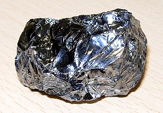
Silicon is a chemical element with the symbol Si and atomic number 14. It is a hard, brittle crystalline solid with a blue-grey metallic lustre, and is a tetravalent metalloid and semiconductor. It is a member of group 14 in the periodic table: carbon is above it; and germanium, tin, lead, and flerovium are below it. It is relatively unreactive. Because of its high chemical affinity for oxygen, it was not until 1823 that Jöns Jakob Berzelius was first able to prepare it and characterize it in pure form. Its oxides form a family of anions known as silicates. Its melting and boiling points of 1414 °C and 3265 °C, respectively, are the second highest among all the metalloids and nonmetals, being surpassed only by boron. Silicon is the eighth most common element in the universe by mass, but very rarely occurs as the pure element in the Earth's crust. It is most widely distributed in space in cosmic dusts, planetoids, and planets as various forms of silicon dioxide (silica) or silicates. More than 90% of the Earth's crust is composed of silicate minerals, making silicon the second most abundant element in the Earth's crust, after oxygen. Silicon is a natural element, and when not previously present has a residence time of about 400 years in the world's oceans.
A semiconductor material has an electrical conductivity value falling between that of a conductor, such as metallic copper, and an insulator, such as glass. Its resistivity falls as its temperature rises; metals behave in the opposite way. Its conducting properties may be altered in useful ways by introducing impurities ("doping") into the crystal structure. When two differently doped regions exist in the same crystal, a semiconductor junction is created. The behavior of charge carriers, which include electrons, ions, and electron holes, at these junctions is the basis of diodes, transistors, and most modern electronics. Some examples of semiconductors are silicon, germanium, gallium arsenide, and elements near the so-called "metalloid staircase" on the periodic table. After silicon, gallium arsenide is the second-most common semiconductor and is used in laser diodes, solar cells, microwave-frequency integrated circuits, and others. Silicon is a critical element for fabricating most electronic circuits.

A semiconductor device is an electronic component that relies on the electronic properties of a semiconductor material for its function. Semiconductor devices have replaced vacuum tubes in most applications. They conduct electric current in the solid state, rather than as free electrons across a vacuum or as free electrons and ions through an ionized gas.
The electron affinity (Eea) of an atom or molecule is defined as the amount of energy released when an electron is attached to a neutral atom or molecule in the gaseous state to form a negative ion.

Epitaxy refers to a type of crystal growth or material deposition in which new crystalline layers are formed with one or more well-defined orientations with respect to the crystalline seed layer. The deposited crystalline film is called an epitaxial film or epitaxial layer. The relative orientation(s) of the epitaxial layer to the seed layer is defined in terms of the orientation of the crystal lattice of each material. For most epitaxial growths, the new layer is usually crystalline and each crystallographic domain of the overlayer must have a well-defined orientation relative to the substrate crystal structure. Epitaxy can involve single-crystal structures, although grain-to-grain epitaxy has been observed in granular films. For most technological applications, single domain epitaxy, which is the growth of an overlayer crystal with one well-defined orientation with respect to the substrate crystal, is preferred. Epitaxy can also play an important role while growing superlattice structures.
In physics, a charge carrier is a particle or quasiparticle that is free to move, carrying an electric charge, especially the particles that carry electric charges in electrical conductors. Examples are electrons, ions and holes. The term is used most commonly in solid state physics. In a conducting medium, an electric field can exert force on these free particles, causing a net motion of the particles through the medium; this is what constitutes an electric current. In conducting media, particles serve to carry charge:

In chemistry and physics, a valence electron is an electron in the outer shell associated with an atom, and that can participate in the formation of a chemical bond if the outer shell is not closed; in a single covalent bond, both atoms in the bond contribute one valence electron in order to form a shared pair.

A p–n junction is a boundary or interface between two types of semiconductor materials, p-type and n-type, inside a single crystal of semiconductor. The "p" (positive) side contains an excess of holes, while the "n" (negative) side contains an excess of electrons in the outer shells of the electrically neutral atoms there. This allows electrical current to pass through the junction only in one direction. The p-n junction is created by doping, for example by ion implantation, diffusion of dopants, or by epitaxy. If two separate pieces of material were used, this would introduce a grain boundary between the semiconductors that would severely inhibit its utility by scattering the electrons and holes.

A high-electron-mobility transistor (HEMT), also known as heterostructure FET (HFET) or modulation-doped FET (MODFET), is a field-effect transistor incorporating a junction between two materials with different band gaps as the channel instead of a doped region. A commonly used material combination is GaAs with AlGaAs, though there is wide variation, dependent on the application of the device. Devices incorporating more indium generally show better high-frequency performance, while in recent years, gallium nitride HEMTs have attracted attention due to their high-power performance. Like other FETs, HEMTs are used in integrated circuits as digital on-off switches. FETs can also be used as amplifiers for large amounts of current using a small voltage as a control signal. Both of these uses are made possible by the FET’s unique current–voltage characteristics. HEMT transistors are able to operate at higher frequencies than ordinary transistors, up to millimeter wave frequencies, and are used in high-frequency products such as cell phones, satellite television receivers, voltage converters, and radar equipment. They are widely used in satellite receivers, in low power amplifiers and in the defense industry.
In semiconductor production, doping is the intentional introduction of impurities into an intrinsic semiconductor for the purpose of modulating its electrical, optical and structural properties. The doped material is referred to as an extrinsic semiconductor. A semiconductor doped to such high levels that it acts more like a conductor than a semiconductor is referred to as a degenerate semiconductor.
In semiconductor physics, the depletion region, also called depletion layer, depletion zone, junction region, space charge region or space charge layer, is an insulating region within a conductive, doped semiconductor material where the mobile charge carriers have been diffused away, or have been forced away by an electric field. The only elements left in the depletion region are ionized donor or acceptor impurities.
An intrinsic (pure) semiconductor, also called an undoped semiconductor or i-type semiconductor, is a pure semiconductor without any significant dopant species present. The number of charge carriers is therefore determined by the properties of the material itself instead of the amount of impurities. In intrinsic semiconductors the number of excited electrons and the number of holes are equal: n = p. This may be the case even after doping the semiconductor, though only if it is doped with both donors and acceptors equally. In this case, n = p still holds, and the semiconductor remains intrinsic, though doped.
Lead telluride is a compound of lead and tellurium (PbTe). It crystallizes in the NaCl crystal structure with Pb atoms occupying the cation and Te forming the anionic lattice. It is a narrow gap semiconductor with a band gap of 0.32 eV. It occurs naturally as the mineral altaite.
An extrinsic semiconductor is one that has been doped; during manufacture of the semiconductor crystal a trace element or chemical called a doping agent has been incorporated chemically into the crystal, for the purpose of giving it different electrical properties than the pure semiconductor crystal, which is called an intrinsic semiconductor. In an extrinsic semiconductor it is these foreign dopant atoms in the crystal lattice that mainly provide the charge carriers which carry electric current through the crystal. The doping agents used are of two types, resulting in two types of extrinsic semiconductor. An electron donor dopant is an atom which, when incorporated in the crystal, releases a mobile conduction electron into the crystal lattice. An extrinsic semiconductor which has been doped with electron donor atoms is called an n-type semiconductor, because the majority of charge carriers in the crystal are negative electrons. An electron acceptor dopant is an atom which accepts an electron from the lattice, creating a vacancy where an electron should be called a hole which can move through the crystal like a positively charged particle. An extrinsic semiconductor which has been doped with electron acceptor atoms is called a p-type semiconductor, because the majority of charge carriers in the crystal are positive holes.

In semiconductor physics, an acceptor is a dopant atom that when added to a semiconductor can form a p-type region.
A Mott transition is a metal-nonmetal transition in condensed matter. Due to electric field screening the potential energy becomes much more sharply (exponentially) peaked around the equilibrium position of the atom and electrons become localized and can no longer conduct a current.
A degenerate semiconductor is a semiconductor with such a high level of doping that the material starts to act more like a metal than as a semiconductor. Unlike non-degenerate semiconductors, these kind of semiconductor do not obey law of mass action, which relates intrinsic carrier concentration with temperature and bandgap.
A dopant, also called a doping agent, is a trace of impurity element that is introduced into a chemical material to alter its original electrical or optical properties. The amount of dopant necessary to cause changes is typically very low. When doped into crystalline substances, the dopant's atoms get incorporated into its crystal lattice. The crystalline materials are frequently either crystals of a semiconductor such as silicon and germanium for use in solid-state electronics, or transparent crystals for use in the production of various laser types; however, in some cases of the latter, noncrystalline substances such as glass can also be doped with impurities.
Monolayer doping (MLD) is a well controlled, wafer-scale surface doping technique first developed at the University of California, Berkeley, in 2007. This work is aimed for attaining controlled doping of semiconductor materials with atomic accuracy, especially at nanoscale, which is not easily obtained by other existing technologies. This technique is currently used for fabricating ultrashallow junctions (USJs) as the heavily doped source/drain (S/D) contacts of metal-oxide-semiconductor field effect transistors (MOSFETs) as well as enabling dopant profiling of nanostructures.
