The Czochralski method, also Czochralski technique or Czochralski process, is a method of crystal growth used to obtain single crystals (monocrystals) of semiconductors (e.g. silicon, germanium and gallium arsenide), metals (e.g. palladium, platinum, silver, gold), salts and synthetic gemstones. The method is named after Polish scientist Jan Czochralski,[1] who invented the method in 1915 while investigating the crystallization rates of metals.[2] He made this discovery by accident: instead of dipping his pen into his inkwell, he dipped it in molten tin, and drew a tin filament, which later proved to be a single crystal.[3] The process remains economically important, as roughly 90% of all modern-day semiconductor devices use material derived from this method.[4]
The method is not limited to production of metal or metalloid crystals. For example, it is used to manufacture very high-purity crystals of salts, including material with controlled isotopic composition, for use in particle physics experiments, with tight controls (part per billion measurements) on confounding metal ions and water absorbed during manufacture.[6]
History
Early developments (1915–1930s)
Jan Czochralski - a Polish chemist invented his method in 1916 at AEG in Germany while investigating the crystallization velocities of metals.[2] His technique—originally reported in 1918—formed the basis for growing single crystals by pulling material from the melt. Until 1923, modifications to the method were confined mainly to Berlin‐based groups.[7]
Shortly thereafter, in 1925, E.P.T. Tyndall's group at the University of Iowa grew zinc crystals using the Czochralski method for nearly a decade; these early crystals reached maximum diameters of about 3.5 mm and lengths of up to 35 cm.
The development of the fundamental process would be completed in 1937 by Henry Walther at Bell Telephone Laboratories.[8] Walther introduced crystal rotation—a technique that compensates for thermal asymmetries—and implemented dynamic cooling control via an adjustable gas stream. His innovations enabled precise control over crystal shape and diameter and allowed the first growth of true bulk crystals, including high-melting-point materials such as sodium chloride. Walther's work laid the foundation for the modern Czochralski process.[7]
Post–World War II revival (1940s–1950s)
The strategic importance of semiconductors following World War II led Gordon Teal, then employed at Bell Labs to revive the Czochralski method for single crystal growth. In the early 1950s, high-quality germanium crystals were grown to meet the emerging demands of transistor technology, and soon after, silicon crystals were produced. This renewed interest marked the beginning of a rapid expansion in the use of the technique in the United States.[7][9]
Global spread and process refinements (late 1950s–present)
The adoption of the Czochralski method expanded internationally in the late 1950s. In Europe, Germany employed the technique for semiconductor crystals as early as 1952, followed by France in 1953, the United Kingdom and Russia in 1956, the Czech Republic in 1957, and finally Switzerland and the Netherlands in 1959. In Japan, the technique began to be used in 1959, with its applications and technical improvements accelerating during the 1960s.[7]
During this period several key process modifications were introduced that further refined the Czochralski method: • The hot-wall technique (circa 1956) reduced evaporation losses from the melt. • The continuous melt feed method (circa 1956) stabilized the melt composition. • The liquid encapsulated Czochralski (LEC) technique (introduced in 1962) enabled the growth of compound semiconductor crystals by suppressing the evaporation of volatile components. • Automatic diameter control using crystal or crucible weighing (introduced in 1972–73) allowed for more precise regulation of crystal dimensions.
These innovations extended the versatility of the Czochralski process, paving the way for industrial-scale production of high-quality single crystals across a wide range of materials.[7]
Application
Monocrystalline silicon (mono-Si) grown by the Czochralski method is often referred to as monocrystalline Czochralski silicon (Cz-Si). It is the basic material in the production of integrated circuits used in computers, TVs, mobile phones and all types of electronic equipment and semiconductor devices.[10] Monocrystalline silicon is also used in large quantities by the photovoltaic industry for the production of conventional mono-Si solar cells. The almost perfect crystal structure yields the highest light-to-electricity conversion efficiency for silicon.
Use of the Czochralski process is not limited to semiconductor materials; it is extensively utilized in the growth of high-quality optical crystals and synthetic gemstones. This method enables the production of large, high-purity crystals suitable for various optical applications. For instance, synthetic alexandrite—a variety of chrysoberyl—is commonly produced using this technique. Additionally, synthetic sapphire (corundum) is frequently grown through the Czochralski process. Furthermore, yttrium aluminium garnet (YAG), an artificial garnet, has been synthesized using this method. YAG crystals are utilized as diamond simulants and in various optical applications, benefiting from the process's ability to produce large, high-purity crystals.[11][12][13]
Semiconductor-grade silicon (only a few parts per million of impurities) is melted in a crucible at 1,425°C (2,597°F; 1,698K), usually made of high-purity quartz. The crucible receives a charge consisting of high-purity polysilicon.[14] Dopant impurity atoms such as boron or phosphorus can be added to the molten silicon in precise amounts to dope the silicon, thus changing it into p-type or n-type silicon, with different electronic properties. A precisely oriented rod-mounted seed crystal is dipped into the molten silicon. The seed crystal's rod is slowly pulled upwards and rotated simultaneously. By precisely controlling the temperature gradients, rate of pulling and speed of rotation, it is possible to extract a large, single-crystal, cylindrical ingot from the melt. Occurrence of unwanted instabilities in the melt can be avoided by investigating and visualizing the temperature and velocity fields during the crystal growth process.[15] This process is normally performed in an inert atmosphere, such as argon, in an inert chamber, such as quartz. The quartz crucible is normally discarded after the process is terminated which normally happens after a single ingot is produced in what is known as a batch process, but it is possible to perform this process continuously, as well as with an applied magnetic field.[16]
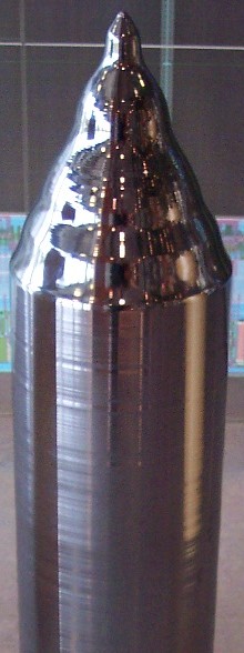
Crystal sizes
Silicon crystal being grown by the Czochralski method at Raytheon, 1956. The induction heating coil is visible, and the end of the crystal is just emerging from the melt. The technician is measuring the temperature with an optical pyrometer. The crystals produced by this early apparatus, used in an early Si plant, were only one inch in diameter.
Due to efficiencies of scale, the semiconductor industry often uses wafers with standardized dimensions, or common wafer specifications. Early on, boules were small, a few centimeters wide. With advanced technology, high-end device manufacturers use 200mm and 300mm diameter wafers. Width is controlled by precise control of temperature, speeds of rotation, and the speed at which the seed holder is withdrawn. The crystal ingots from which wafers are sliced can be up to 2 metres in length, weighing several hundred kilograms. Larger wafers allow improvements in manufacturing efficiency, as more chips can be fabricated on each wafer, with lower relative loss, so there has been a steady drive to increase silicon wafer sizes. The next step up, 450mm, was scheduled for introduction in 2018.[17] Silicon wafers are typically about 0.2–0.75mm thick, and can be polished to great flatness for making integrated circuits or textured for making solar cells.
Incorporating impurities
A puller rod with seed crystal for growing single-crystal silicon by the Czochralski methodCrucibles used in Czochralski methodCrucible after being used
When silicon is grown by the Czochralski method, the melt is contained in a silica (quartz) crucible. During growth, the walls of the crucible dissolve into the melt and Czochralski silicon therefore contains oxygen at a typical concentration of 1018 cm−3 . Oxygen impurities can have beneficial or detrimental effects. Carefully chosen annealing conditions can give rise to the formation of oxygen precipitates. These have the effect of trapping unwanted transition metal impurities in a process known as gettering, improving the purity of surrounding silicon. However, formation of oxygen precipitates at unintended locations can also destroy electrical structures. Additionally, oxygen impurities can improve the mechanical strength of silicon wafers by immobilising any dislocations which may be introduced during device processing. It was experimentally shown in the 1990s that the high oxygen concentration is also beneficial for the radiation hardness of silicon particle detectors used in harsh radiation environment (such as CERN's LHC/HL-LHC projects).[18][19] Therefore, radiation detectors made of Czochralski- and magnetic Czochralski-silicon are considered to be promising candidates for many future high-energy physics experiments.[20][21] It has also been shown that the presence of oxygen in silicon increases impurity trapping during post-implantation annealing processes.[22]
However, oxygen impurities can react with boron in an illuminated environment, such as that experienced by solar cells. This results in the formation of an electrically active boron–oxygen complex that detracts from cell performance. Module output drops by approximately 3% during the first few hours of light exposure.[23]
Mathematical form
Impurity concentration in the final solid is given by where C and C0 are (respectively) the initial and final concentration, V and V0 the initial and final volume, and k the segregation coefficient associated with impurities at the melting phase transition. This follows from the fact that impurities are removed from the melt when an infinitesimal volume dV freezes.[24]
↑ Paweł Tomaszewski, "Jan Czochralski i jego metoda. Jan Czochralski and his method" (in Polish and English), Oficyna Wydawnicza ATUT, Wrocław–Kcynia 2003, ISBN83-89247-27-5
↑ CERN RD50 Status Report 2004, CERN-LHCC-2004-031 and LHCC-RD-005 and cited literature therein
↑ Harkonen, J; Tuovinen, E; Luukka, P; Tuominen, E; Li, Z; Ivanov, A; Verbitskaya, E; Eremin, V; Pirojenko, A; Riihimaki, I.; Virtanen, A. (2005). "Particle detectors made of high-resistivity Czochralski silicon". Nuclear Instruments and Methods in Physics Research Section A: Accelerators, Spectrometers, Detectors and Associated Equipment. 541 (1–2): 202–207. Bibcode:2005NIMPA.541..202H. CiteSeerX10.1.1.506.2366. doi:10.1016/j.nima.2005.01.057.
↑ Custer, J. S.; Polman, A.; Van Pinxteren, H. M. (1994). "Erbium in crystal silicon: Segregation and trapping during solid phase epitaxy of amorphous silicon". Journal of Applied Physics. 75 (6): 2809. Bibcode:1994JAP....75.2809C. doi:10.1063/1.356173.
This page is based on this Wikipedia article Text is available under the CC BY-SA 4.0 license; additional terms may apply. Images, videos and audio are available under their respective licenses.