Shaping processes in crystal growth

Last updated
Crystallization
Process-of-Crystallization-200px.png
Fundamentals
Concepts
Methods and technology

Shaping processes in crystal growth are a collection of techniques for growing bulk crystals of a defined shape from a melt, usually by constraining the shape of the liquid meniscus by means of a mechanical shaper. Crystals are commonly grown as fibers, solid cylinders, hollow cylinders (or tubes), and sheets (or plates). More complex shapes such as tubes with a complex cross section, and domes have also been produced. [1] Using a shaping process can produce a near net shape crystal and reduce the manufacturing cost for crystals which are composed of very expensive or difficult to machine materials.

Contents

List of shaping processes

Edge-defined film-fed growth

Edge-defined film-fed growth or EFG was developed for sapphire growth in the late 1960s by Harold LaBelle and A. Mlavsky at Tyco Industries. [4] A shaper (also referred to as a die) having dimensions approximately equal to the crystal to be grown rests above the surface of the melt which is contained in a crucible. Capillary action feeds liquid material to a slit at the center of the shaper. When a seed crystal is touched to the liquid film and raised upwards, a single crystal forms at the interface between the solid seed and the liquid film. By continuing to pull the seed upwards, the crystal expands as a liquid film forms between the crystal and the top surface of the shaper. When the film reaches the edges of the shaper, the final crystal shape matches that of the shaper.

The exact dimensions of the crystal will deviate from the dimensions of the shaper because every material has a characteristic growth angle, the angle formed at the triple interface between the solid crystal, liquid film, and the atmosphere. [5] Because of the growth angle, varying the height of the meniscus (i.e. the thickness of the liquid film) will change the dimensions of the crystal. The meniscus height is affected by pulling speed and crystallization rate. The crystallization rate depends on the temperature gradient above the shaper, which is determined by the configuration of the hot-zone of the crystal growth furnace, and the power applied to the heating elements during growth. The difference in thermal expansion coefficients between the shaper material and the crystal material can also cause appreciable size differences between the shaper and the crystal at room temperature for crystals grown at high temperatures.

The shaper material should be non-reactive with both the melt and growth atmosphere, and should be wet by the melt. [6]

It is possible to grow multiple crystals from a single crucible using the EFG technique, for example by growing many parallel sheets.

Applications

Sapphire: EFG is used to grow large plates of sapphire, primarily for use as robust infrared windows for defense and other applications. Windows about 7 mm thick x 300  mm wide x 500 mm long are produced. [7] The shaper is typically made from molybdenum.

Silicon: EFG was used in the 2000s by Schott Solar to produce silicon sheets for solar photovoltaic panels, by pulling a thin-walled (~250-300 μm) octagon with faces 12.5 cm on a side and diameter about 38 cm, about 5–6 m long. [8] The shaper is typically made from graphite.

Other oxides: Many high melting-point oxides have been grown by EFG, among them Ga2O3, LiNbO3, and Nd3+:(LuxGd1−x)3Ga5O12 (Nd:LGGG). [9] Often an iridium shaper is used.

Horizontal ribbon growth

Horizontal ribbon growth or HRG is a method developed and patented by William Shockley in 1959 for silicon growth. [2] [3] By this method a thin crystalline sheet is pulled horizontally from the top of a crucible. The melt level must be constantly replenished in order to keep the surface of the melt at the same height as the edge of the crucible from which the sheet is being pulled. By blowing a cooling gas at the surface of the growing sheet, very high growth rates (>400 mm/min) can be achieved. [10] The method relies on the solid crystal floating on the surface of the melt, which works because solid silicon is less dense than liquid silicon.

Micro-pulling-down

The micro-pulling-down or µ-PD technique uses a small round opening in the bottom of the crucible to pull a crystalline fiber downward. Hundreds of different crystalline materials have been grown by this technique.

A variation called pendant drop growth or PDG uses a slot in the bottom of the crucible to produce crystalline sheets in a similar manner. [5]

Stepanov technique

The Stepanov technique was developed by A.V. Stepanov in the Soviet Union after 1950. [1] The method involves pulling a crystal vertically through a shaper located at the surface of the melt. The shaper is not necessarily fed by a capillary channel as in EFG. [11] The shaper material may be wetted or non-wetted by the melt, as opposed to EFG where the shaper material is wetted. [6] The technique has been used to grow metal, semiconductor, and oxide crystals.

Czochralski growth using a floating shaper known as a "coracle" was done for some III-V semiconductors prior to the development of advanced control-systems for diameter control. [12]

String ribbon

The string ribbon method, also known as dendritic web or edge-supported pulling, has been used to grow semiconductor sheets including indium antimonide, gallium arsenide, germanium, and silicon. [13] A seed crystal with the width and thickness matching the sheet to be grown is dipped into the top surface of the melt. Strings of a suitable material are fixed to the vertical edges of the seed and extend down through holes in the bottom of the crucible to a spool. As the seed is raised, string is continuously fed through the melt and a liquid film forms between the seed, the strings, and the melt. The film crystallizes to the seed, forming a sheet or ribbon.

Related Research Articles

<span class="mw-page-title-main">Gemstone</span> Piece of mineral crystal used to make jewelry

A gemstone is a piece of mineral crystal which, in cut and polished form, is used to make jewelry or other adornments. However, certain rocks and occasionally organic materials that are not minerals are also used for jewelry and are therefore often considered to be gemstones as well. Most gemstones are hard, but some soft minerals are used in jewelry because of their luster or other physical properties that have aesthetic value. Rarity and notoriety are other characteristics that lend value to gemstones.

<span class="mw-page-title-main">Zone melting</span> Purification process by moving a molten zone along a metal bar

Zone melting is a group of similar methods of purifying crystals, in which a narrow region of a crystal is melted, and this molten zone is moved along the crystal. The molten region melts impure solid at its forward edge and leaves a wake of purer material solidified behind it as it moves through the ingot. The impurities concentrate in the melt, and are moved to one end of the ingot. Zone refining was invented by John Desmond Bernal and further developed by William G. Pfann in Bell Labs as a method to prepare high-purity materials, mainly semiconductors, for manufacturing transistors. Its first commercial use was in germanium, refined to one atom of impurity per ten billion, but the process can be extended to virtually any solute–solvent system having an appreciable concentration difference between solid and liquid phases at equilibrium. This process is also known as the float zone process, particularly in semiconductor materials processing.

<span class="mw-page-title-main">Czochralski method</span> Method of crystal growth

The Czochralski method, also Czochralski technique or Czochralski process, is a method of crystal growth used to obtain single crystals of semiconductors, metals, salts and synthetic gemstones. The method is named after Polish scientist Jan Czochralski, who invented the method in 1915 while investigating the crystallization rates of metals. He made this discovery by accident: instead of dipping his pen into his inkwell, he dipped it in molten tin, and drew a tin filament, which later proved to be a single crystal. The method is still used in over 90 percent of all electronics in the world that use semiconductors.

<span class="mw-page-title-main">Ingot</span> Piece of relatively pure metal

An ingot is a piece of relatively pure material, usually metal, that is cast into a shape suitable for further processing. In steelmaking, it is the first step among semi-finished casting products. Ingots usually require a second procedure of shaping, such as cold/hot working, cutting, or milling to produce a useful final product. Non-metallic and semiconductor materials prepared in bulk form may also be referred to as ingots, particularly when cast by mold based methods. Precious metal ingots can be used as currency, or as a currency reserve, as with gold bars.

<span class="mw-page-title-main">Epitaxy</span> Crystal growth process relative to the substrate

Epitaxy refers to a type of crystal growth or material deposition in which new crystalline layers are formed with one or more well-defined orientations with respect to the crystalline seed layer. The deposited crystalline film is called an epitaxial film or epitaxial layer. The relative orientation(s) of the epitaxial layer to the seed layer is defined in terms of the orientation of the crystal lattice of each material. For most epitaxial growths, the new layer is usually crystalline and each crystallographic domain of the overlayer must have a well-defined orientation relative to the substrate crystal structure. Epitaxy can involve single-crystal structures, although grain-to-grain epitaxy has been observed in granular films. For most technological applications, single domain epitaxy, which is the growth of an overlayer crystal with one well-defined orientation with respect to the substrate crystal, is preferred. Epitaxy can also play an important role while growing superlattice structures.

<span class="mw-page-title-main">Bridgman–Stockbarger method</span> Method of crystallization

The Bridgman–Stockbarger method, or Bridgman–Stockbarger technique, is named after Harvard physicist Percy Williams Bridgman (1882–1961) and MIT physicist Donald C. Stockbarger (1895–1952). The method includes two similar but distinct techniques primarily used for growing boules, but which can be used for solidifying polycrystalline ingots as well.

<span class="mw-page-title-main">Single crystal</span> Material with a continuous, unbroken crystal lattice

In materials science, a single crystal is a material in which the crystal lattice of the entire sample is continuous and unbroken to the edges of the sample, with no grain boundaries. The absence of the defects associated with grain boundaries can give monocrystals unique properties, particularly mechanical, optical and electrical, which can also be anisotropic, depending on the type of crystallographic structure. These properties, in addition to making some gems precious, are industrially used in technological applications, especially in optics and electronics.

<span class="mw-page-title-main">Lanthanum gallium silicate</span> Chemical compound

Lanthanum gallium silicate (referred to as LGS in this article), also known as langasite, has a chemical formula of the form A3BC3D2O14, where A, B, C and D indicate particular cation sites. A is a decahedral (Thomson cube) site coordinated by 8 oxygen atoms. B is octahedral site coordinated by 6 oxygen atoms, and C and D are tetrahedral sites coordinated by 4 oxygen atoms. In this material, lanthanum occupied the A-sites, gallium the B, C and half of D-sites, and, silicon the other half of D-sites.

Synthetic alexandrite is an artificially grown crystalline variety of chrysoberyl, composed of beryllium aluminum oxide (BeAl2O4).

Chemical beam epitaxy (CBE) forms an important class of deposition techniques for semiconductor layer systems, especially III-V semiconductor systems. This form of epitaxial growth is performed in an ultrahigh vacuum system. The reactants are in the form of molecular beams of reactive gases, typically as the hydride or a metalorganic. The term CBE is often used interchangeably with metal-organic molecular beam epitaxy (MOMBE). The nomenclature does differentiate between the two processes, however. When used in the strictest sense, CBE refers to the technique in which both components are obtained from gaseous sources, while MOMBE refers to the technique in which the group III component is obtained from a gaseous source and the group V component from a solid source.

<span class="mw-page-title-main">Verneuil method</span> Manufacturing process of synthetic gemstones

The Verneuil method, also called flame fusion, was the first commercially successful method of manufacturing synthetic gemstones, developed in the late 1883 by the French chemist Auguste Verneuil. It is primarily used to produce the ruby, sapphire and padparadscha varieties of corundum, as well as the diamond simulants rutile, strontium titanate and spinel. The principle of the process involves melting a finely powdered substance using an oxyhydrogen flame, and crystallising the melted droplets into a boule. The process is considered to be the founding step of modern industrial crystal growth technology, and remains in wide use to this day.

<span class="mw-page-title-main">Melt spinning</span>

Melt spinning is a metal forming technique that is typically used to form thin ribbons of metal or alloys with a particular atomic structure.

Diffraction topography is a imaging technique based on Bragg diffraction. Diffraction topographic images ("topographies") record the intensity profile of a beam of X-rays diffracted by a crystal. A topography thus represents a two-dimensional spatial intensity mapping of reflected X-rays, i.e. the spatial fine structure of a Laue reflection. This intensity mapping reflects the distribution of scattering power inside the crystal; topographs therefore reveal the irregularities in a non-ideal crystal lattice. X-ray diffraction topography is one variant of X-ray imaging, making use of diffraction contrast rather than absorption contrast which is usually used in radiography and computed tomography (CT). Topography is exploited to a lesser extends with neutrons, and has similarities to dark field imaging in the electron microscope community.

Selective area epitaxy is the local growth of epitaxial layer through a patterned amorphous dielectric mask (typically SiO2 or Si3N4) deposited on a semiconductor substrate. Semiconductor growth conditions are selected to ensure epitaxial growth on the exposed substrate, but not on the dielectric mask. SAE can be executed in various epitaxial growth methods such as molecular beam epitaxy (MBE), metalorganic vapour phase epitaxy (MOVPE) and chemical beam epitaxy (CBE). By SAE, semiconductor nanostructures such as quantum dots and nanowires can be grown to their designed places.

Monocrystalline silicon, more often called single-crystal silicon, in short mono c-Si or mono-Si, is the base material for silicon-based discrete components and integrated circuits used in virtually all modern electronic equipment. Mono-Si also serves as a photovoltaic, light-absorbing material in the manufacture of solar cells.

<span class="mw-page-title-main">Laser-heated pedestal growth</span>

Laser-heated pedestal growth (LHPG) or laser floating zone (LFZ) is a crystal growth technique. A narrow region of a crystal is melted with a powerful CO2 or YAG laser. The laser and hence the floating zone, is moved along the crystal. The molten region melts impure solid at its forward edge and leaves a wake of purer material solidified behind it. This technique for growing crystals from the melt is used in materials research.

<span class="mw-page-title-main">Micro-pulling-down</span> Crystal growth technique

The micro-pulling-down (μ-PD) method is a crystal growth technique based on continuous transport of the melted substance through micro-channel(s) made in a crucible bottom. Continuous solidification of the melt is progressed on a liquid/solid interface positioned under the crucible. In a steady state, both the melt and the crystal are pulled-down with a constant velocity.

<span class="mw-page-title-main">Yttrium borides</span> Chemical compound

Yttrium boride refers to a crystalline material composed of different proportions of yttrium and boron, such as YB2, YB4, YB6, YB12, YB25, YB50 and YB66. They are all gray-colored, hard solids having high melting temperatures. The most common form is the yttrium hexaboride YB6. It exhibits superconductivity at relatively high temperature of 8.4 K and, similar to LaB6, is an electron cathode. Another remarkable yttrium boride is YB66. It has a large lattice constant (2.344 nm), high thermal and mechanical stability, and therefore is used as a diffraction grating for low-energy synchrotron radiation (1–2 keV).

A rapidly increasing list of graphene production techniques have been developed to enable graphene's use in commercial applications.
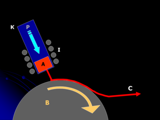
<span class="mw-page-title-main">Kyropoulos method</span> Method of bulk crystal growth used to obtain single crystals

The Kyropoulos method, KY method, or Kyropoulos technique, is a method of bulk crystal growth used to obtain single crystals.

References

  1. 1 2 Dobrovinskaya, Elena R., Leonid A. Lytvynov, and Valerian Pishchik. Sapphire: material, manufacturing, applications. Springer Science & Business Media, 2009. ISBN   0387856943
  2. 1 2 Daggolu, Parthiv (December 2013). "Thermal-Capillary Analysis of the Horizontal Ribbon Growth of Solar Silicon" (PDF). University of Minnesota.
  3. 1 2 US 3031275,Shockley, William,"Process for growing single crystals",published 1962-04-24
  4. Robichaud, Joseph L.; Harris, Daniel C.; Goodman, William A. (2009). "A century of sapphire crystal growth: origin of the EFG method". In Robichaud, Joseph L.; Goodman, William A. (eds.). Optical Materials and Structures Technologies IV. Vol. 7425. pp. 74250P. doi:10.1117/12.824452. ISSN   0277-786X.
  5. 1 2 Duffar, Thierry (2015). "Capillarity and Shape Stability in Crystal Growth from the Melt". In Rudolph, Peter (ed.). Handbook of Crystal Growth Vol. IIB (2nd ed.). Elsevier B.V. pp. 758–789. doi:10.1016/B978-0-444-63303-3.00019-5. ISBN   9780444633033.
  6. 1 2 Surek, T.; Coriell, S.R.; Chalmers, B. (1980). "The growth of shaped crystals from the melt". Journal of Crystal Growth. 50 (1): 21–32. doi:10.1016/0022-0248(80)90227-4. ISSN   0022-0248.
  7. "CLASS Sapphire Sheets". Saint-Gobain. Retrieved 25 January 2018.
  8. Mackintosh, B; Seidl, A; Ouellette, M; Bathey, B; Yates, D; Kelejs, J (25 January 2006). "Large silicon crystal hollow-tube growth by the edge-defined film-fed growth (EFG) method". Journal of Crystal Growth. 287 (2): 428–432. doi:10.1016/j.jcrysgro.2005.11.058.
  9. Mu, Wenxiang; Jia, Zhitai; Yin, Yanru; Hu, Qiangqiang; Li, Yang; Tao, Xutang (2017). "Growth of homogeneous Nd:LGGG single crystal plates by edge-defined film-fed growth method". Journal of Crystal Growth. 478: 17–21. doi:10.1016/j.jcrysgro.2017.08.007. ISSN   0022-0248.
  10. Kudo, B. (1980). "Improvements in the Horizontal Ribbon Growth technique for single crystal silicon". Journal of Crystal Growth. 50 (1): 247–259. doi:10.1016/0022-0248(80)90248-1.
  11. Tatartchenko, Vitali (2010). "Shaped Crystal Growth: TPS Brief History". In Dhanaraj, Govindhan; et al. (eds.). Springer Handbook of Crystal Growth. Springer. pp. 537–541.
  12. Winkler, Jan; Neubert, Michael (2015). "Automation of Crystal Growth from Melt". In Rudolph, Peter (ed.). Handbook of Crystal Growth (2nd ed.). Elsevier B.V. p. 1153. doi:10.1016/B978-0-444-63303-3.00028-6. ISBN   9780444633033.
  13. Seidensticker, R.G.; Hopkins, R.H. (1980). "Silicon ribbon growth by the dendritic web process". Journal of Crystal Growth. 50 (1): 221–235. doi:10.1016/0022-0248(80)90246-8. ISSN   0022-0248.