
A protocrystalline phase is a distinct phase occurring during crystal growth, which evolves into a microcrystalline form. The term is typically associated with silicon films in optical applications such as solar cells. [1]
A protocrystalline phase is a distinct phase occurring during crystal growth, which evolves into a microcrystalline form. The term is typically associated with silicon films in optical applications such as solar cells. [1]
Amorphous silicon (a-Si) is a popular solar cell material owing to its low cost and ease of production. Owing to its disordered structure (Urbach tail), its absorption extends to the energies below the band gap, resulting in a wide-range spectral response; however, it has a relatively low solar cell efficiency. Protocrystalline Si (pc-Si:H) also has a relatively low absorption near the band gap, owing to its more ordered crystalline structure. Thus, protocrystalline and amorphous silicon can be combined in a tandem solar cell, where the top thin layer of a-Si:H absorbs short-wavelength light whereas the underlying protocrystalline silicon layer absorbs the longer wavelengths [2]

Gallium arsenide (GaAs) is a III-V direct band gap semiconductor with a zinc blende crystal structure.

Nanocrystalline silicon (nc-Si), sometimes also known as microcrystalline silicon (μc-Si), is a form of porous silicon. It is an allotropic form of silicon with paracrystalline structure—is similar to amorphous silicon (a-Si), in that it has an amorphous phase. Where they differ, however, is that nc-Si has small grains of crystalline silicon within the amorphous phase. This is in contrast to polycrystalline silicon (poly-Si) which consists solely of crystalline silicon grains, separated by grain boundaries. The difference comes solely from the grain size of the crystalline grains. Most materials with grains in the micrometre range are actually fine-grained polysilicon, so nanocrystalline silicon is a better term. The term Nanocrystalline silicon refers to a range of materials around the transition region from amorphous to microcrystalline phase in the silicon thin film. The crystalline volume fraction is another criterion to describe the materials in this transition zone.

The term quantum efficiency (QE) may apply to incident photon to converted electron (IPCE) ratio of a photosensitive device, or it may refer to the TMR effect of a magnetic tunnel junction.

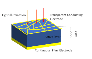
A solar cell or photovoltaic cell is an electronic device that converts the energy of light directly into electricity by means of the photovoltaic effect. It is a form of photoelectric cell, a device whose electrical characteristics vary when it is exposed to light. Individual solar cell devices are often the electrical building blocks of photovoltaic modules, known colloquially as "solar panels". Almost all commercial PV cells consist of crystalline silicon, with a market share of 95%. Cadmium telluride thin-film solar cells account for the remainder. The common single-junction silicon solar cell can produce a maximum open-circuit voltage of approximately 0.5 to 0.6 volts.

A quantum dot solar cell (QDSC) is a solar cell design that uses quantum dots as the captivating photovoltaic material. It attempts to replace bulk materials such as silicon, copper indium gallium selenide (CIGS) or cadmium telluride (CdTe). Quantum dots have bandgaps that are adjustable across a wide range of energy levels by changing their size. In bulk materials, the bandgap is fixed by the choice of material(s). This property makes quantum dots attractive for multi-junction solar cells, where a variety of materials are used to improve efficiency by harvesting multiple portions of the solar spectrum.

Building-integrated photovoltaics (BIPV) are photovoltaic materials that are used to replace conventional building materials in parts of the building envelope such as the roof, skylights, or façades. They are increasingly being incorporated into the construction of new buildings as a principal or ancillary source of electrical power, although existing buildings may be retrofitted with similar technology. The advantage of integrated photovoltaics over more common non-integrated systems is that the initial cost can be offset by reducing the amount spent on building materials and labor that would normally be used to construct the part of the building that the BIPV modules replace. In addition, BIPV allows for more widespread solar adoption when the building's aesthetics matter and traditional rack-mounted solar panels would disrupt the intended look of the building.

Multi-junction (MJ) solar cells are solar cells with multiple p–n junctions made of different semiconductor materials. Each material's p-n junction will produce electric current in response to different wavelengths of light. The use of multiple semiconducting materials allows the absorbance of a broader range of wavelengths, improving the cell's sunlight to electrical energy conversion efficiency.
An organic solar cell (OSC) or plastic solar cell is a type of photovoltaic that uses organic electronics, a branch of electronics that deals with conductive organic polymers or small organic molecules, for light absorption and charge transport to produce electricity from sunlight by the photovoltaic effect. Most organic photovoltaic cells are polymer solar cells.
TEL Solar, formerly Oerlikon Solar, is a manufacturer of production equipment for the manufacturing of thin-film silicon cells, headquartered in Trübbach, Switzerland, near the border to Liechtenstein. The Japanese electronics and semiconductor company Tokyo Electron acquired the company of about 650 employees from OC Oerlikon in November 2012.
The portmanteau micromorph is a combination of the words microcrystalline and amorphous. It is used for a type of silicon based multijunction thin-film solar cell.

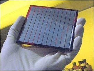
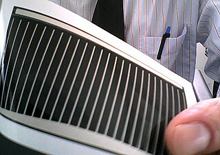
Thin-film solar cells are a type of solar cell made by depositing one or more thin layers of photovoltaic material onto a substrate, such as glass, plastic or metal. Thin-film solar cells are typically a few nanometers (nm) to a few microns (μm) thick–much thinner than the wafers used in conventional crystalline silicon (c-Si) based solar cells, which can be up to 200 μm thick. Thin-film solar cells are commercially used in several technologies, including cadmium telluride (CdTe), copper indium gallium diselenide (CIGS), and amorphous thin-film silicon.
A copper indium gallium selenide solar cell is a thin-film solar cell used to convert sunlight into electric power. It is manufactured by depositing a thin layer of copper indium gallium selenide solid solution on glass or plastic backing, along with electrodes on the front and back to collect current. Because the material has a high absorption coefficient and strongly absorbs sunlight, a much thinner film is required than of other semiconductor materials.
A plasmonic-enhanced solar cell, commonly referred to simply as plasmonic solar cell, is a type of solar cell that converts light into electricity with the assistance of plasmons, but where the photovoltaic effect occurs in another material.

Crystalline silicon or (c-Si) Is the crystalline forms of silicon, either polycrystalline silicon, or monocrystalline silicon. Crystalline silicon is the dominant semiconducting material used in photovoltaic technology for the production of solar cells. These cells are assembled into solar panels as part of a photovoltaic system to generate solar power from sunlight.

Wahid Shams-Kolahi is a scientist and an electrical engineer who is known for his research in photovoltaic-related technologies.
There are currently many research groups active in the field of photovoltaics in universities and research institutions around the world. This research can be categorized into three areas: making current technology solar cells cheaper and/or more efficient to effectively compete with other energy sources; developing new technologies based on new solar cell architectural designs; and developing new materials to serve as more efficient energy converters from light energy into electric current or light absorbers and charge carriers.
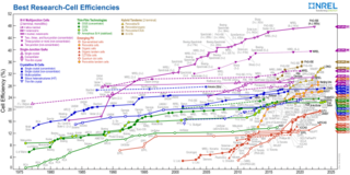
Solar-cell efficiency is the portion of energy in the form of sunlight that can be converted via photovoltaics into electricity by the solar cell.

Amorphous silicon (a-Si) is the non-crystalline form of silicon used for solar cells and thin-film transistors in LCDs.
The Urbach Energy, or Urbach Edge, is a parameter typically denoted , with dimensions of energy, used to quantify energetic disorder in the band edges of a semiconductor. It is evaluated by fitting the absorption coefficient as a function of energy to an exponential function. It is often used to describe electron transport in structurally disordered semiconductors such as hydrogenated amorphous silicon.

Heterojunction solar cells (HJT), variously known as Silicon heterojunctions (SHJ) or Heterojunction with Intrinsic Thin Layer (HIT), are a family of photovoltaic cell technologies based on a heterojunction formed between semiconductors with dissimilar band gaps. They are a hybrid technology, combining aspects of conventional crystalline solar cells with thin-film solar cells.
| | This crystallography-related article is a stub. You can help Wikipedia by expanding it. |