This article needs to be updated. The reason given is: industry and production figures, in particular, are very out of date. Please help update this article to reflect recent events or newly available information.(June 2024)
Left side: solar cells made of polycrystalline silicon Right side: polysilicon rod (top) and chunks (bottom)
Polycrystalline silicon, or multicrystalline silicon, also called polysilicon, poly-Si, or mc-Si, is a high purity, polycrystalline form of silicon, used as a raw material by the solar photovoltaic and electronics industry.
Polysilicon is produced from metallurgical grade silicon by a chemical purification process, called the Siemens process. This process involves distillation of volatile silicon compounds, and their decomposition into silicon at high temperatures. An emerging, alternative process of refinement uses a fluidized bed reactor, which is lower cost.[1] The photovoltaic industry also produces upgraded metallurgical-grade silicon (UMG-Si), using metallurgical instead of chemical purification processes for lower cost at the expense of purity.[2][3][4][5] When produced for the electronics industry, polysilicon contains impurity levels of less than one part per billion (ppb), while polycrystalline solar grade silicon (SoG-Si) is generally less pure. In the 2010's, production shifted toward China, with China-based companies accounting for seven of the top ten producers and around 90% of total worldwide production capacity of approximately 1,400,000 MT. German, US and South Korea companies account for the remainder.[6]
Polycrystalline solar cells, often called multi-crystalline panels, are highly cost-effective, budget-friendly, and durable photovoltaic devices made by melting multiple silicon fragments together. Recognizable by their square shape and blue, speckled, mosaic-like appearance, they typically have an efficiency of 14% to 18%. These panels are ideal for large-scale, cost-conscious solar projects. The polysilicon feedstock – large rods from the Siemens process, usually broken into chunks of specific sizes and packaged in clean rooms before shipment[7] – is directly cast into multicrystalline ingots which are large square blocks weighing around 800 kg[8] for making solar wafers[9] or submitted as-is to a recrystallization process to grow single crystal boules usually with the Czochralski method.[10][9] The boules are then sliced into thin silicon wafers and used for the production of solar cells, integrated circuits and other semiconductor devices.
Polysilicon consists of small crystals, also known as crystallites, giving the material its typical metal flake effect. While polysilicon and multisilicon are often used as synonyms, multicrystalline usually refers to crystals larger than one millimetre. Multicrystalline solar cells are the most common type of solar cells in the fast-growing PV market and consume most of the worldwide produced polysilicon. About 5 tons of polysilicon is required to manufacture one 1 megawatt (MW) of conventional solar modules.[11][citation needed] Polysilicon is distinct from monocrystalline silicon and amorphous silicon.
Vs monocrystalline silicon
Comparing polycrystalline (left) to monocrystalline (right) solar cells
In single-crystal silicon, also known as monocrystalline silicon, the crystalline framework is homogeneous, which can be recognized by an even external colouring.[12] The entire sample is one single, continuous and unbroken crystal as its structure contains no grain boundaries. Large single crystals are rare in nature and can also be difficult to produce in the laboratory (see also recrystallisation). In contrast, in an amorphous structure the order in atomic positions is limited to short range.
Polycrystalline and paracrystalline phases are composed of a number of smaller crystals or crystallites. Polycrystalline silicon (or semi-crystalline silicon, polysilicon, poly-Si, or simply "poly") is a material consisting of multiple small silicon crystals. Polycrystalline cells can be recognized by a visible grain, a "metal flake effect". Semiconductor grade (also solar grade) polycrystalline silicon is converted to single-crystal silicon – meaning that the randomly associated crystallites of silicon in polycrystalline silicon are converted to a large single crystal. Single-crystal silicon is used to manufacture most Si-based microelectronic devices. Polycrystalline silicon can be as much as 99.9999% pure.[13] Ultra-pure poly is used in the semiconductor industry, starting from poly rods that are two to three meters in length resulting from the Siemens process. In the microelectronics industry (semiconductor industry), poly is used at both the macro and micro scales. Single crystals are grown using the Czochralski, zone melting and Bridgman–Stockbarger methods. The Czochralski method often uses polysilicon as the starting material.[14]
A rod of semiconductor-grade polysilicon vía the Siemens process
At the component level, polysilicon has long been used as the conducting gate material in MOSFET and CMOS processing technologies. For these technologies, it is deposited using low-pressure chemical-vapour deposition (LPCVD) reactors at high temperatures and is usually heavily doped n-type or p-type.
More recently, intrinsic and doped polysilicon is being used in large-area electronics as the active and/or doped layers in thin-film transistors. Although it can be deposited by LPCVD, plasma-enhanced chemical vapour deposition (PECVD), or solid-phase crystallization of amorphous silicon in certain processing regimes, these processes still require relatively high temperatures of at least 300°C. These temperatures make deposition of polysilicon possible for glass substrates but not for plastic substrates.
The deposition of polycrystalline silicon on plastic substrates is motivated by the desire to be able to manufacture digital displays on flexible screens. Therefore, a relatively new technique called laser crystallization has been devised to crystallize a precursor amorphous silicon (a-Si) material on a plastic substrate without melting or damaging the plastic. Short, high-intensity ultravioletlaser pulses are used to heat the deposited a-Si material to above the melting point of silicon, without melting the entire substrate.
The molten silicon will then crystallize as it cools. By precisely controlling the temperature gradients, researchers have been able to grow very large grains, of up to hundreds of micrometers in size in the extreme case, although grain sizes of 10 nanometers to 1 micrometer are also common. In order to create devices on polysilicon over large-areas, however, a crystal grain size smaller than the device feature size is needed for homogeneity of the devices. Another method to produce poly-Si at low temperatures is metal-induced crystallization where an amorphous-Si thin film can be crystallized at temperatures as low as 150°C if annealed while in contact of another metal film such as aluminium, gold, or silver.
Polysilicon has many applications in VLSI manufacturing. One of its primary uses is as gate electrode material for MOS devices. A polysilicon gate's electrical conductivity may be increased by depositing a metal (such as tungsten) or a metal silicide (such as tungsten silicide) over the gate. Polysilicon may also be employed as a resistor, a conductor, or as an ohmic contact for shallow junctions, with the desired electrical conductivity attained by doping the polysilicon material.
One major difference between polysilicon and a-Si is that the mobility of the charge carriers of the polysilicon can be orders of magnitude larger and the material also shows greater stability under electric field and light-induced stress. This allows more complex, high-speed circuitry to be created on the glass substrate along with the a-Si devices, which are still needed for their low-leakage characteristics. When polysilicon and a-Si devices are used in the same process, this is called hybrid processing. A complete polysilicon active layer process is also used in some cases where a small pixel size is required, such as in projection displays.
Polycrystalline silicon is the key feedstock in the crystalline silicon based photovoltaic industry and used for the production of conventional solar cells. For the first time, in 2006, over half of the world's supply of polysilicon was being used by PV manufacturers.[15] The solar industry was severely hindered by a shortage in supply of polysilicon feedstock and was forced to idle about a quarter of its cell and module manufacturing capacity in 2007.[16] Only twelve factories were known to produce solar-grade polysilicon in 2008; however, by 2013 the number increased to over 100 manufacturers.[17] Monocrystalline silicon is higher priced and a more efficient semiconductor than polycrystalline as it has undergone additional recrystallization via the Czochralski method. Trichlorosilane is used to create high purity electronic grade (poly)silicon (EGS) from metallurgical grade (poly)silicon (MGS) which is produced from quartzite. EGS is used for silicon photovoltaics[18] and is necessary for the Czochralski method of wafer production used in integrated circuits.[19]
Deposition methods
Polysilicon deposition, or the process of depositing a layer of polycrystalline silicon on a semiconductor wafer, is achieved by the chemical decomposition of silane (SiH4) at high temperatures of 580 to 650°C. This pyrolysis process releases hydrogen.
Polysilicon layers can be deposited using 100% silane at a pressure of 25–130Pa (0.19–0.98Torr) or with 20–30% silane (diluted in nitrogen) at the same total pressure. Both of these processes can deposit polysilicon on 10–200 wafers per run, at a rate of 10–20nm/min and with thickness uniformities of ±5%. Critical process variables for polysilicon deposition include temperature, pressure, silane concentration, and dopant concentration. Wafer spacing and load size have been shown to have only minor effects on the deposition process. The rate of polysilicon deposition increases rapidly with temperature, since it follows Arrhenius behavior, that is deposition rate = A·exp(–qEa/kT) where q is electron charge and k is the Boltzmann constant. The activation energy (Ea) for polysilicon deposition is about 1.7eV. Based on this equation, the rate of polysilicon deposition increases as the deposition temperature increases. There will be a minimum temperature, however, wherein the rate of deposition becomes faster than the rate at which unreacted silane arrives at the surface. Beyond this temperature, the deposition rate can no longer increase with temperature, since it is now being hampered by lack of silane from which the polysilicon will be generated. Such a reaction is then said to be "mass-transport-limited". When a polysilicon deposition process becomes mass-transport-limited, the reaction rate becomes dependent primarily on reactant concentration, reactor geometry, and gas flow.
When the rate at which polysilicon deposition occurs is slower than the rate at which unreacted silane arrives, then it is said to be surface-reaction-limited. A deposition process that is surface-reaction-limited is primarily dependent on reactant concentration and reaction temperature. Deposition processes must be surface-reaction-limited because they result in excellent thickness uniformity and step coverage. A plot of the logarithm of the deposition rate against the reciprocal of the absolute temperature in the surface-reaction-limited region results in a straight line whose slope is equal to –qEa/k.
At reduced pressure levels for VLSI manufacturing, polysilicon deposition rate below 575°C is too slow to be practical. Above 650°C, poor deposition uniformity and excessive roughness will be encountered due to unwanted gas-phase reactions and silane depletion. Pressure can be varied inside a low-pressure reactor either by changing the pumping speed or changing the inlet gas flow into the reactor. If the inlet gas is composed of both silane and nitrogen, the inlet gas flow, and hence the reactor pressure, may be varied either by changing the nitrogen flow at constant silane flow, or changing both the nitrogen and silane flow to change the total gas flow while keeping the gas ratio constant. Recent investigations have shown that e-beam evaporation, followed by SPC (if needed) can be a cost-effective and faster alternative for producing solar-grade poly-Si thin films.[21] Modules produced by such method are shown to have a photovoltaic efficiency of ~6%.[22]
Polysilicon doping, if needed, is also done during the deposition process, usually by adding phosphine, arsine, or diborane. Adding phosphine or arsine results in slower deposition, while adding diborane increases the deposition rate. The deposition thickness uniformity usually degrades when dopants are added during deposition.
Schematic diagram of the traditional Siemens and the fluidized bed reactor purification process
The Siemens process is the most commonly used method of polysilicon production, especially for electronics,[23] with close to 75% of the world's production using this process as of 2005.[24] It has been used since the 1950s with the advent of the semiconductor industry, for semiconductor devices with silicon.[2] The Siemens process is named after the Siemens company, which invented the process in 1954.[25]
The process converts metallurgical-grade Si, of approximately 98% purity, to SiHCl3 (Trichlorosilane) and then to silicon in a reactor, thus removing transition metal and dopant impurities.[23] The process is relatively expensive and slow.[23] The power consumption of the process is high. Due to this, 17 alternatives have been investigated, however the Siemens process prevails specially due to its use at Chinese production sites.[26] However tube filaments have gained traction.[27]
It is a type of chemical vapor deposition process.[28] The process begins with tall, thin silicon wires or filaments 7mm in diameter and around 2.5m tall, square in cross section made via the Czochralski method from monocrystalline silicon ingots. The wires are etched with hydrofluoric acid to remove oxides from the surface and are bridged at the top by setting silicon wires. They are installed on electrodes. The reactor is closed and an electric current is passed through the wires via the electrodes to heat them to 1150°C. The outside of the reactor is cooled with water. Hydrochloric acid can be used as a catalyst. The trichlorosilane is introduced together with hydrogen and deposits on the hot surface of the wires by interacting with the catalyst and the process stops once the wires reach a diameter of 120mm, forming the rods in 46 hours. Another 24 hours are required for installing wires, etching them and harvesting the rods for a total of 60 hours per batch. Factories usually have redundant power supplies for this process. Then the rods are harvested, removed from the reactor, broken into chunks and packed in nitrogen or argon filled bags for shipment. Most large factories produce the trichlorosilane on site. It is best to remove the reaction products from the reactor as soon as they are created so the reactor has an exhaust for silicon tetrachloride, hydrogen, trichlorosilane, dichlorosilane and hydrochloric acid.
FBR process
In the FBR process, small silicon particles called seeds are continuously introduced into the reactor, while silane and hydrogen are introduced. The particles are moved by gases to make them behave like a fluid. In a chemical vapor deposition process within the reactor, silane becomes silicon and deposits onto the seeds, making them larger, which are then removed from the reactor. The FBR process is estimated to consume one order of magnitude less power than the Siemens process, at 5 to 10 Kwh/Kg of silicon. The exhaust of the FBR reactor is hydrogen and unreacted silane.[29][30] As of 2021 the Siemens process is almost exclusively used as the FBR process only has a 1.9% market share.[31]
Upgraded metallurgical-grade silicon
Upgraded metallurgical-grade (UMG) silicon (also known as UMG-Si) for solar cells is being produced as a low cost alternative to polysilicon created by the Siemens process. UMG-Si greatly reduces impurities in a variety of ways that require less equipment and energy than the Siemens process.[32] It is about 99% pure which is three or more orders of magnitude less pure and about 10 times less expensive than polysilicon ($1.70 to $3.20 per kg from 2005 to 2008 compared to $40 to $400 per kg for polysilicon). It has the potential to provide nearly-as-good solar cell efficiency at 1/5 the capital expenditure, half the energy requirements, and less than $15/kg.[33]
In 2008, several companies were touting the potential of UMG-Si, but in 2010 the credit crisis greatly lowered the cost of polysilicon and several UMG-Si producers put plans on hold.[34][35][36][37][38][39] The Siemens process will remain the dominant form of production for years to come due to more efficiently implementing the Siemens process. GT Solar claims a new Siemens process can produce at $27/kg and may reach $20/kg in 5 years. GCL-Poly expects production costs to be $20/kg by end of 2011.[40] Elkem Solar estimates their UMG costs to be $25/kg, with a capacity of 6,000 tonnes by the end of 2010. Calisolar expects UMG technology to produce at $12/kg in 5 years with boron at 0.3ppm and phosphorus at 0.6ppm.[41] At $50/kg and 7.5g/W, module manufacturers spend $0.37/W for the polysilicon. For comparison, if a CdTe manufacturer pays spot price for tellurium ($420/kg in April 2010) and has a 3μm thickness, their cost would be 10 times less, $0.037/Watt. At 0.1g/W and $31/ozt for silver, polysilicon solar producers spend $0.10/W on silver.[42]
Q-Cells, Canadian Solar, and Calisolar have used Timminco UMG. Timminco is able to produce UMG-Si with 0.5 ppm boron for $21/kg but were sued by shareholders because they had expected $10/kg.[43] RSI and Dow Corning have also been in litigation over UMG-Si technology.[44]
Potential applications
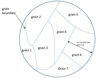
A picture of grain boundaries for polysilicon. Each grain is crystalline over the width of the grain. The grain boundary separates the grains where the adjoining grain is at a different orientation from its neighbor. The grain boundary separates regions of different crystal structure thus serving as a center for recombination. 'd' here is a characteristic grain size, which should be maximized for maximum solar cell efficiency. Typical values of d are about 1 micrometre.
Currently, polysilicon is commonly used for the conducting gate materials in semiconductor devices such as MOSFETs; however, it has potential for large-scale photovoltaic devices.[45][46] The abundance, stability, and low toxicity of silicon, combined with the low cost of polysilicon relative to single crystals makes this variety of material attractive for photovoltaic production.[46] Grain size has been shown to have an effect on the efficiency of polycrystalline solar cells. Solar cell efficiency increases with grain size. This effect is due to reduced recombination in the solar cell. Recombination, which is a limiting factor for current in a solar cell, occurs more prevalently at grain boundaries, see figure 1.[46]
The resistivity, mobility, and free-carrier concentration in monocrystalline silicon vary with doping concentration of the single crystal silicon. Whereas the doping of polycrystalline silicon does have an effect on the resistivity, mobility, and free-carrier concentration, these properties strongly depend on the polycrystalline grain size, which is a physical parameter that the material scientist can manipulate.[46] Through the methods of crystallization to form polycrystalline silicon, an engineer can control the size of the polycrystalline grains which will vary the physical properties of the material.
Novel ideas
The use of polycrystalline silicon in the production of solar cells requires less material and therefore provides higher profits and increased manufacturing throughput. Polycrystalline silicon does not need to be deposited on a silicon wafer to form a solar cell, rather it can be deposited on other, cheaper materials, thus reducing the cost. Not requiring a silicon wafer alleviates the silicon shortages occasionally faced by the microelectronics industry.[47] An example of not using a silicon wafer is crystalline silicon on glass (CSG) materials.[47]
A primary concern in the photovoltaics industry is cell efficiency. However, sufficient cost savings from cell manufacturing can be suitable to offset reduced efficiency in the field, such as the use of larger solar cell arrays compared with more compact/higher efficiency designs. Designs such as CSG are attractive because of a low cost of production even with reduced efficiency.[47] Higher efficiency devices yield modules that occupy less space and are more compact; however, the 5–10% efficiency of typical CSG devices still makes them attractive for installation in large central-service stations, such as a power station.[47] The issue of efficiency versus cost is a value decision of whether one requires an "energy dense" solar cell or sufficient area is available for the installation of less expensive alternatives. For instance, a solar cell used for power generation in a remote location might require a more highly efficient solar cell than one used for low-power applications, such as solar accent lighting or pocket calculators, or near established power grids.
Manufacturers
This section needs to be updated. Please help update this article to reflect recent events or newly available information.(April 2021)
Capacity
Polysilicon production by country in 2013 (company headquarters, not location of facility). World total of 227,000 tonnes.[48]
China (36.1%)
USA (25.9%)
South Korea (11.4%)
Germany (21.6%)
Japan (4.90%)
Chemical processing at a P.S.T. polysilicon plant
The polysilicon manufacturing market has been growing rapidly. According to DigiTimes, in July 2011, the total polysilicon production in 2010 was 209,000 tons. First-tier suppliers account for 64% of the market while China-based polysilicon firms have 30% of market share. The total production is likely to increase 37.4% to 281,000 tons by end of 2011.[49] For 2012, EETimes Asia predicts 328,000 tons production with only 196,000 tons of demand, with spot prices expected to fall 56%. While good for renewable energy prospects, the subsequent drop in price could be brutal for manufacturers.[50] As of late 2012, SolarIndustryMag reports a capacity of 385,000 tons will be reached by yearend 2012.[51]
As of 2010, as established producers (mentioned below) expand their capacities, additional newcomers – many from Asia – are moving into the market. Even long-time players in the field have recently had difficulties expanding plant production. It is yet unclear which companies will be able to produce at costs low enough to be profitable after the steep drop in spot-prices of the last months.[52][53]
Leading producers
Wacker's projected its total hyperpure-polysilicon production capacity to increase to 67,000 metric tons by 2014, due to its new polysilicon-production facility in Cleveland, Tennessee (US) with an annual capacity of 15,000 metric tons.[54][55][56]
Largest polysilicon producers in 2013 (market-share in%)
Prices of polysilicon are often divided into two categories, contract and spot prices, and higher purity commands higher prices. While in booming installation times, price rally occurs in polysilicon. Not only spot prices surpass contract prices in the market; but it is also hard to acquire enough polysilicon. Buyers will accept down payment and long-term agreements to acquire a large enough volume of polysilicon. On the contrary, spot prices will be below contract prices once the solar PV installation is in a down trend. In late 2010, booming installation brought up the spot prices of polysilicon. In the first half of 2011, prices of polysilicon kept strong owing to the FIT policies of Italy. The solar PV price survey and market research firm, PVinsights,[69] reported that the prices of polysilicon might be dragged down by lack of installation in the second half of 2011.[70] As recently as 2008 prices were over $400/kg spiking from levels around $200/kg, while seen falling to $15/kg in 2013.[71]
Dumping
The Chinese government accused United States and South Korean manufacturers of predatory pricing or "dumping". As a consequence, in 2013 it imposed import tariffs of as much as 57 percent on polysilicon shipped from these two countries in order to stop the product from being sold below cost.[72]
Waste
Due to the rapid growth in manufacturing in China and the lack of regulatory controls, there have been reports of the dumping of waste silicon tetrachloride.[73] Normally the waste silicon tetrachloride is recycled but this adds to the cost of manufacture as it needs to be heated to 1,800°F (980°C).
↑Dasilva-Villanueva, N.; Catalán-Gómez, S.; Fuertes Marrón, D.; Torres, J.J.; García-Corpas, M.; del Cañizo, C. (January 2022). "Reduction of trapping and recombination in upgraded metallurgical grade silicon: Impact of phosphorous diffusion gettering". Solar Energy Materials and Solar Cells. 234 111410. arXiv:2106.15926. Bibcode:2022SEMSC.23411410D. doi:10.1016/j.solmat.2021.111410.
↑Méndez, Laura; Forniés, Eduardo; Garrain, Daniel; Pérez Vázquez, Antonio; Souto, Alejandro; Vlasenko, Timur (1 October 2021). "Upgraded metallurgical grade silicon and polysilicon for solar electricity production: A comparative life cycle assessment". Science of the Total Environment. 789 147969. arXiv:2102.11571. Bibcode:2021ScTEn.78947969M. doi:10.1016/j.scitotenv.2021.147969. PMID34082204. S2CID232013656.
↑Morgan, D. V.; Board, K. (1991). An Introduction To Semiconductor Microtechnology (2nded.). Chichester, West Sussex, England: John Wiley & Sons. p.27. ISBN0-471-92478-4.
↑C. Becker, "Microstructure and photovoltaic performance of polycrystalline silicon thin films on temperature-stable ZnO:Al layers". J. Appl. Phys. 106, 084506 (2009), DOI:10.1063/1.3240343
↑Lv, Qinghui; Yuan, Xingping; Guo, Lijie; Zhao, Dan; Ma, Wenhui; Xie, Gang; Hou, Yanqing; Shen, Jinglei; Yang, Ni (May 2025). "Advances in production and optimization of electronic-grade polysilicon: A review of modified Siemens and silane methods". Solar Energy Materials and Solar Cells. 283 113446. Bibcode:2025SEMSC.28313446L. doi:10.1016/j.solmat.2025.113446.
↑Streetman, B. G. & Banerjee, S. (2000), Solid State Electronic Devices (5thed.), New Jersey: Prentice Hall, ISBN0-13-025538-6
1234Ghosh, Amal K.; Fishman, Charles & Feng, Tom (1980), "Theory of the electrical and photovoltaic properties of polycrystalline silicon", Journal of Applied Physics, 51 (1): 446, Bibcode:1980JAP....51..446G, doi:10.1063/1.327342
This page is based on this Wikipedia article Text is available under the CC BY-SA 4.0 license; additional terms may apply. Images, videos and audio are available under their respective licenses.