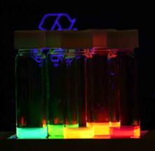
Hybrid solar cell

Last updated

Hybrid solar cells combine advantages of both organic and inorganic semiconductors. Hybrid photovoltaics have organic materials that consist of conjugated polymers that absorb light as the donor and transport holes. [1] Inorganic materials in hybrid cells are used as the acceptor and electron transporter in the structure. The hybrid photovoltaic devices have a potential for not only low-cost by roll-to-roll processing but also for scalable solar power conversion.

Contents

Theory

Solar cells are devices that convert sunlight into electricity by the photovoltaic effect. Electrons in a solar cell absorb photon energy in sunlight which excites them to the conduction band from the valence band. This generates a hole-electron pair, which is separated by a potential barrier (such as a p-n junction), and induces a current. Organic solar cells use organic materials in their active layers. Molecular, polymer, and hybrid organic photovoltaics are the main kinds of organic photovoltaic devices currently studied.

Hybrid solar cell

Figure 1. Energy diagram of the donor and acceptor. The conduction band of the acceptor is lower than the LUMO of the polymer, allowing for transfer of the electron. Chargeseperation mike.JPG
Figure 1. Energy diagram of the donor and acceptor. The conduction band of the acceptor is lower than the LUMO of the polymer, allowing for transfer of the electron.

In hybrid solar cells, an organic material is mixed with a high electron transport material to form the photoactive layer. [2] The two materials are assembled together in a heterojunction-type photoactive layer, which can have a greater power conversion efficiency than a single material. [3] One of the materials acts as the photon absorber and exciton donor. The other material facilitates exciton dissociation at the junction. Charge is transferred and then separated after an exciton created in the donor is delocalized on a donor-acceptor complex. [4] [5]

The acceptor material needs a suitable energy offset to the binding energy of the exciton to the absorber. Charge transfer is favorable if the following condition is satisfied: [6]

where superscripts A and D refer to the acceptor and donor respectively, EA is the electron affinity, and U the coulombic binding energy of the exciton on the donor. An energy diagram of the interface is shown in figure 1. In commonly used photovoltaic polymers such as MEH-PPV, the exciton binding energy ranges from 0.3 eV to 1.4 eV. [7]

The energy required to separate the exciton is provided by the energy offset between the LUMOs or conduction bands of the donor and acceptor. [3] After dissociation, the carriers are transported to the respective electrodes through a percolation network.

The average distance an exciton can diffuse through a material before annihilation by recombination is the exciton diffusion length. This is short in polymers, on the order of 5–10 nanometers. [6] The time scale for radiative and non-radiative decay is from 1 picosecond to 1 nanosecond. [8] Excitons generated within this length close to an acceptor would contribute to the photocurrent.

Figure 2. Two different structures of heterojunctions, a) phase separated bi-layer and b) bulk heterojunction. The bulk heterojunction allows for more interfacial contact between the two phases, which is beneficial for the nanoparticle-polymer compound as it provides more surface area for charge transfer. Heterojunction mike.JPG
Figure 2. Two different structures of heterojunctions, a) phase separated bi-layer and b) bulk heterojunction. The bulk heterojunction allows for more interfacial contact between the two phases, which is beneficial for the nanoparticle-polymer compound as it provides more surface area for charge transfer.

To deal with the problem of the short exciton diffusion length, a bulk heterojunction structure is used rather than a phase-separated bilayer. Dispersing the particles throughout the polymer matrix creates a larger interfacial area for charge transfer to occur. [3] Figure 2 displays the difference between a bilayer and a bulk heterojunction.

Types of interfaces and structures

Controlling the interface of inorganic-organic hybrid solar cells can increase the efficiency of the cells. This increased efficiency can be achieved by increasing the interfacial surface area between the organic and the inorganic to facilitate charge separation and by controlling the nanoscale lengths and periodicity of each structure so that charges are allowed to separate and move toward the appropriate electrode without recombining. The three main nanoscale structures used are mesoporous inorganic films infused with electron-donating organic, alternatining inorganic-organic lamellar structures, and nanowire structures.

Mesoporous films

Mesoporous films have been used for a relatively high-efficiency hybrid solar cell. [9] The structure of mesoporous thin film solar cells usually includes a porous inorganic that is saturated with organic surfactant. The organic absorbs light, and transfers electrons to the inorganic semiconductor (usually a transparent conducting oxide), which then transfers the electron to the electrode. Problems with these cells include their random ordering and the difficulty of controlling their nanoscale structure to promote charge conduction.

Ordered lamellar films

Recently, the use of alternating layers of organic and inorganic compounds has been controlled through electrodeposition-based self-assembly. [10] This is of particular interest because it has been shown that the lamellar structure and periodicity of the alternating organic-inorganic layers can be controlled through solution chemistry. To produce this type of cell with practical efficiencies, larger organic surfactants that absorb more of the visible spectrum must be deposited between the layers of electron-accepting inorganic.

Films of ordered nanostructures

Researchers have been able to grow nanostructure-based solar cells that use ordered nanostructures like nanowires or nanotubes of inorganic surrounding by electron-donating organics utilizing self-organization processes. Ordered nanostructures offer the advantage of directed charge transport and controlled phase separation between donor and acceptor materials. [11] The nanowire-based morphology offers reduced internal reflection, facile strain relaxation and increased defect tolerance. The ability to make single-crystalline nanowires on low-cost substrates such as aluminum foil and to relax strain in subsequent layers removes two more major cost hurdles associated with high-efficiency cells. There have been rapid increases in efficiencies of nanowire-based solar cells and they seem to be one of the most promising nanoscale solar hybrid technologies. [12]

Fundamental challenge factors

Hybrid cell efficiency must be increased to start large-scale manufacturing. Three factors affect efficiency. [2] [13] First, the bandgap should be reduced to absorb red photons, which contain a significant fraction of the energy in the solar spectrum. Current organic photovoltaics have shown 70% of quantum efficiency for blue photons. Second, contact resistance between each layer in the device should be minimized to offer higher fill factor and power conversion efficiency. Third, charge-carrier mobility should be increased to allow the photovoltaics to have thicker active layers while minimizing carrier recombination and keeping the series resistance of the device low.

Types of hybrid solar cells

Polymer–nanoparticle composite

Nanoparticles are a class of semiconductor materials whose size in at least one dimension ranges from 1 to 100 nanometers, on the order of exciton wavelengths. This size control creates quantum confinement and allows for the tuning of optoelectronic properties, such as band gap and electron affinity. Nanoparticles also have a large surface area to volume ratio, which presents more area for charge transfer to occur. [14]

The photoactive layer can be created by mixing nanoparticles into a polymer matrix. Solar devices based on polymer-nanoparticle composites most resemble polymer solar cells. In this case, the nanoparticles take the place of the fullerene based acceptors used in fully organic polymer solar cells. Hybrid solar cells based upon nanoparticles are an area of research interest because nanoparticles have several properties that could make them preferable to fullerenes, such as:

Structure and processing

Figure 3. Four different structures of nanoparticles, which have at least 1 dimension in the 1-100 nm range, retaining quantum confinement. Left is a nanocrystal, next to it is nanorod, third is tetrapod, and right is hyperbranched. Nanoparticles mike.JPG
Figure 3. Four different structures of nanoparticles, which have at least 1 dimension in the 1–100 nm range, retaining quantum confinement. Left is a nanocrystal, next to it is nanorod, third is tetrapod, and right is hyperbranched.

For polymers used in this device, hole mobilities are greater than electron mobilities, so the polymer phase is used to transport holes. The nanoparticles transport electrons to the electrode. [14]

The interfacial area between the polymer phase and the nanoparticles needs to be large. This is achieved by dispersing the particles throughout the polymer matrix. However, the nanoparticles need to be interconnected to form percolation networks for electron transport, which occurs by hopping events. [14]

Efficiency is affected by aspect ratio, geometry, and volume fraction of the nanoparticles. Nanoparticle structures include nanocrystals, nanorods, and hyperbranched structures. [3] Figure 3 contains a picture of each structure. Different structures change the conversion efficiency by effecting nanoparticle dispersion in the polymer and providing pathways for electron transport.

The nanoparticle phase is required to provide a pathway for the electrons to reach the electrode. By using nanorods instead of nanocrystals, the hopping event from one crystal to another can be avoided. [14]

Fabrication methods include mixing the two materials in a solution and spin-coating it onto a substrate, and solvent evaporation (sol-gel). Most of these methods do not involve high-temperature processing. Annealing increases order in the polymer phase, increasing conductivity. However, annealing for too long causes the polymer domain size to increase, eventually making it larger than the exciton diffusion length, and possibly allowing some of the metal from the contact to diffuse into the photoactive layer, reducing the efficiency of the device. [3] [14]

Materials

Inorganic semiconductor nanoparticles used in hybrid cells include CdSe (size ranges from 6–20 nm), ZnO, TiO, and PbS. Common polymers used as photo materials have extensive conjugation and are also hydrophobic. Their efficiency as a photo-material is affected by the HOMO level position and the ionization potential, which directly affects the open circuit voltage and the stability in air. The most common polymers used are P3HT (poly (3-hexylthiophene)), and M3H-PPV (poly[2-methoxy, 5-(2′-ethyl-hexyloxy)-p-phenylenevinylene)]). P3HT has a bandgap of 2.1 eV and M3H-PPV has a bandgap of ~2.4 eV. These values correspond with the bandgap of CdSe, 2.10 eV. The electron affinity of CdSe ranges from 4.4 to 4.7 eV. When the polymer used is MEH-PPV, which has an electron affinity of 3.0 eV, the difference between the electron affinities is large enough to drive electron transfer from the CdSe to the polymer. CdSe also has a high electron mobility (600 cm2·V−1·s−1). [3] [6]

Performance values

The highest demonstrated efficiency is 3.2%, based upon a PCPDTBT polymer donor and CdSe nanoparticle acceptor. The device exhibited a short circuit current of 10.1 mA·cm−2, an open circuit voltage of .68 V, and a fill factor of .51. [16]

Challenges

Hybrid solar cells need increased efficiencies and stability over time before commercialization is feasible. In comparison to the 2.4% of the CdSe-PPV system, silicon photodevices have power conversion efficiencies greater than 20%.

Problems include controlling the amount of nanoparticle aggregation as the photolayer forms. The particles need to be dispersed in order to maximize interface area, but need to aggregate to form networks for electron transport. The network formation is sensitive to the fabrication conditions. Dead end pathways can impede flow. A possible solution is implementing ordered heterojunctions, where the structure is well controlled. [14]

The structures can undergo morphological changes over time, namely phase separation. Eventually, the polymer domain size will be greater than the carrier diffusion length, which lowers performance. [3]

Even though the nanoparticle bandgap can be tuned, it needs to be matched with the corresponding polymer. The 2.0 eV bandgap of CdSe is larger than an ideal bandgap of 1.4 for absorbance of light. [14]

The nanoparticles involved are typically colloids, which are stabilized in solution by ligands. The ligands decrease device efficiency because they serve as insulators which impede interaction between the donor and nanoparticle acceptor as well as decreasing the electron mobility. Some, but not complete success has been had by exchanging the initial ligands for pyridine or another short chain ligand. [15]

Hybrid solar cells exhibit material properties inferior to those of bulk silicon semiconductors. The carrier mobilities are much smaller than that of silicon. Electron mobility in silicon is 1000 cm2·V−1·s−1, compared to 600 cm2·V−1·s−1 in CdSe, and less than 10 cm2·V−1·s−1 in other quantum dot materials. Hole mobility in MEH-PPV is 0.1 cm2·V−1·s−1, while in silicon it is 450 cm2·V−1·s−1. [14]

Carbon nanotubes

Carbon nanotubes (CNTs) have high electron conductivity, high thermal conductivity, robustness, and flexibility. Field emission displays (FED), strain sensors, and field effect transistors (FET) using CNTs have been demonstrated. [17] [18] [19] Each application shows the potential of CNTs for nanoscale devices and for flexible electronics applications. Photovoltaic applications have also been explored for this material.

Mainly, CNTs have been used as either the photo-induced exciton carrier transport medium impurity within a polymer-based photovoltaic layer or as the photoactive (photon-electron conversion) layer. Metallic CNT is preferred for the former application, while semiconducting CNT is preferred for the later.

Efficient carrier transport medium

Device diagram for CNT as efficient carrier transport medium. Cntpolymer hj.JPG
Device diagram for CNT as efficient carrier transport medium.

To increase the photovoltaic efficiency, electron-accepting impurities must be added to the photoactive region. By incorporating CNTs into the polymer, dissociation of the exciton pair can be accomplished by the CNT matrix. The high surface area (~1600 m2/g) [20] of CNTs offers a good opportunity for exciton dissociation. The separated carriers within the polymer-CNT matrix are transported by the percolation pathways of adjacent CNTs, providing the means for high carrier mobility and efficient charge transfer. The factors of performance of CNT-polymer hybrid photovoltaics are low compared to those of inorganic photovoltaics. SWNT in P3OT semiconductor polymer demonstrated open circuit voltage (Voc) of below 0.94 V, with short circuit current (Isc) of 0.12 mA/cm2. [20]

Metal nanoparticles may be applied to the exterior of CNTs to increase the exciton separation efficiency. The metal provides a higher electric field at the CNT-polymer interface, accelerating the exciton carriers to transfer them more effectively to the CNT matrix. In this case, Voc = 0.3396 V and Isc = 5.88 mA/cm2. The fill factor is 0.3876%, and the white light conversion factor 0.775%. [21]

Photoactive matrix layer

CNT may be used as a photovoltaic device not only as an add-in material to increase carrier transport, but also as the photoactive layer itself. [22] The semiconducting single walled CNT (SWCNT) is a potentially attractive material for photovoltaic applications for the unique structural and electrical properties. SWCNT has high electric conductivity (100 times that of copper) and shows ballistic carrier transport, greatly decreasing carrier recombination. [23] The bandgap of the SWCNT is inversely proportional to the tube diameter, [23] which means that SWCNT may show multiple direct bandgaps matching the solar spectrum.

A strong built-in electric field in SWCNT for efficient photogenerated electron-hole pair separation has been demonstrated by using two asymmetrical metal electrodes with high and low work functions. The open circuit voltage (Voc) is 0.28 V, with short circuit current (Isc) 1.12 nA·cm−2 with an incident light source of 8.8 W·cm−2. The resulting white light conversion factor is 0.8%. [22]

Challenges

Several challenges must be addressed for CNT to be used in photovoltaic applications. CNT degrades over time in an oxygen-rich environment. The passivation layer required to prevent CNT oxidation may reduce the optical transparency of the electrode region and lower the photovoltaic efficiency.

Challenges as efficient carrier transport medium

Additional challenges involve the dispersion of CNT within the polymer photoactive layer. The CNT is required to be well dispersed within the polymer matrix to form charge-transfer-efficient pathways between the excitons and the electrode [21]

Challenges as photoactive matrix layer

Challenges of CNT for the photoactive layer include its lack of capability to form a p-n junction, due to the difficulty of doping certain segments of a CNT. (A p-n junction creates an internal built-in potential, providing a pathway for efficient carrier separation within the photovoltaic.) To overcome this difficulty, energy band bending has been done by the use of two electrodes of different work functions. A strong built-in electric field covering the whole SWCNT channel is formed for high-efficiency carrier separation. The oxidation issue with CNT is more critical for this application. Oxidized CNTs have a tendency to become more metallic, and so less useful as a photovoltaic material. [24]

Dye-sensitized

Dye-sensitized solar cells consists of a photo-sensitized anode, an electrolyte, and a photo-electrochemical system. Hybrid solar cells based on dye-sensitized solar cells are formed with inorganic materials (TiO2) and organic materials.

Materials

Hybrid solar cells based on dye-sensitized solar cells are fabricated by dye-absorbed inorganic materials and organic materials. TiO2 is the preferred inorganic material since this material is easy to synthesize and acts as a n-type semiconductor due to the donor-like oxygen vacancies. However, titania only absorbs a small fraction of the UV spectrum. Molecular sensitizers (dye molecules) attached to the semiconductor surface are used to collect a greater portion of the spectrum. In the case of titania dye-sensitized solar cells, a photon absorbed by a dye-sensitizer molecule layer induces electron injection into the conduction band of titania, resulting in current flow. However, short diffusion length (diffusivity, Dn≤10−4cm2/s) in titania dye-sensitized solar cells decrease the solar-to-energy conversion efficiency. To enhance diffusion length (or carrier lifetime), a variety of organic materials are attached to the titania.

Fabrication scheme

Dye-sensitized photoelectrochemical cell (Grätzel cell)
Fig. 5. Schematic representation of electron-hole generation and recombination Dyeelectron kh.JPG
Fig. 5. Schematic representation of electron-hole generation and recombination

TiO2 nanoparticles are synthesized in several tens of nanometer scales (~100 nm). In order to make a photovoltaic cell, molecular sensitizers (dye molecules) are attached to the titania surface. The dye-absorbed titania is finally enclosed by a liquid electrolyte. This type of dye-sensitized solar cell is also known as a Grätzel cell. [25] Dye-sensitized solar cell has a disadvantage of a short diffusion length. Recently, supermolecular or multifunctional sensitizers have been investigated so as to enhance carrier diffusion length. [26] For example, a dye chromophore has been modified by the addition of secondary electron donors. Minority carriers (holes in this case) diffuse to the attached electron donors to recombine. Therefore, electron-hole recombination is retarded by the physical separation between the dye–cation moiety and the TiO2 surface, as shown in Fig. 5. Finally, this process raises the carrier diffusion length, resulting in the increase of carrier lifetime.

Solid-state dye sensitized solar cell

Mesoporous materials contain pores with diameters between 2 and 50 nm. A dye-sensitized mesoporous film of TiO2 can be used for making photovoltaic cells and this solar cell is called a ‘solid-state dye sensitized solar cell’. The pores in mesoporous TiO2 thin film are filled with a solid hole-conducting material such as p-type semiconductors or organic hole conducting material. Replacing the liquid electrolyte in Grätzel's cells with a solid charge-transport material can be beneficial. The process of electron-hole generation and recombination is the same as Grätzel cells. Electrons are injected from photoexcited dye into the conduction band of titania and holes are transported by a solid charge transport electrolyte to an electrode. Many organic materials have been tested to obtain a high solar-to-energy conversion efficiency in dye synthesized solar cells based on mesoporous titania thin film. [27]

Efficiency factors

Efficiency factors demonstrated for dye-sensitized solar cells are

ParametersTypes of dye sensitized solar cells
Grätzel cellSolid-state
Efficiency (%)~ 10–11~ 4
Voc (V)~ 0.7~ 0.40
Jsc (mA/cm2)~ 20~ 9.10
Fill factor~ 0.67~ 0.6
Source:

Challenges

Liquid organic electrolytes contain highly corrosive iodine, leading to problems of leakage, sealing, handling, dye desorption, and maintenance. Much attention is now focused on the electrolyte to address these problems.

For solid-state dye sensitized solar cells, the first challenge originates from disordered titania mesoporous structures. Mesoporous titania structures should be fabricated with well-ordered titania structures of uniform size (~ 10 nm). The second challenge comes from developing the solid electrolyte, which is required to have these properties:

  1. The electrolyte should be transparent to the visible spectrum (wide band gap).
  2. Fabrication should be possible for depositing the solid electrolyte without degrading the dye molecule layer on titania.
  3. The LUMO of the dye molecule should be higher than the conduction band of titania.
  4. Several p-type semiconductors tend to crystallize inside the mesoporous titania films, destroying the dye molecule-titania contact. Therefore, the solid electrolyte needs to be stable during operation.

Nanostructured inorganic — small molecules

In 2008, scientists were able to create a nanostructured lamellar structure that provides an ideal design for bulk heterojunction solar cells. [28] The observed structure is composed of ZnO and small, conducting organic molecules, which co-assemble into alternating layers of organic and inorganic components. This highly organized structure, which is stabilized by π-π stacking between the organic molecules, allows for conducting pathways in both the organic and inorganic layers. The thicknesses of the layers (about 1–3 nm) are well within the exciton diffusion length, which ideally minimizes recombination among charge carriers. This structure also maximizes the interface between the inorganic ZnO and the organic molecules, which enables a high chromophore loading density within the structure. Due to the choice of materials, this system is non-toxic and environmentally friendly, unlike many other systems which use lead or cadmium.

Although this system has not yet been incorporated into a photovoltaic device, preliminary photoconductivity measurements have shown that this system exhibits among the highest values measured for organic, hybrid, and amorphous silicon photoconductors, and so, offers promise in creating efficient hybrid photovoltaic devices.

Related Research Articles

<span class="mw-page-title-main">Band gap</span> Energy range in a solid where no electron states exist

In solid-state physics and solid-state chemistry, a band gap, also called a bandgap or energy gap, is an energy range in a solid where no electronic states exist. In graphs of the electronic band structure of solids, the band gap refers to the energy difference between the top of the valence band and the bottom of the conduction band in insulators and semiconductors. It is the energy required to promote an electron from the valence band to the conduction band. The resulting conduction-band electron are free to move within the crystal lattice and serve as charge carriers to conduct electric current. It is closely related to the HOMO/LUMO gap in chemistry. If the valence band is completely full and the conduction band is completely empty, then electrons cannot move within the solid because there are no available states. If the electrons are not free to move within the crystal lattice, then there is no generated current due to no net charge carrier mobility. However, if some electrons transfer from the valence band to the conduction band, then current can flow. Therefore, the band gap is a major factor determining the electrical conductivity of a solid. Substances having large band gaps are generally insulators, those with small band gaps are semiconductor, and conductors either have very small band gaps or none, because the valence and conduction bands overlap to form a continuous band.

Organic semiconductors are solids whose building blocks are pi-bonded molecules or polymers made up by carbon and hydrogen atoms and – at times – heteroatoms such as nitrogen, sulfur and oxygen. They exist in the form of molecular crystals or amorphous thin films. In general, they are electrical insulators, but become semiconducting when charges are either injected from appropriate electrodes, upon doping or by photoexcitation.

<span class="mw-page-title-main">Dye-sensitized solar cell</span> Type of thin-film solar cell

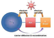
A dye-sensitized solar cell is a low-cost solar cell belonging to the group of thin film solar cells. It is based on a semiconductor formed between a photo-sensitized anode and an electrolyte, a photoelectrochemical system. The modern version of a dye solar cell, also known as the Grätzel cell, was originally co-invented in 1988 by Brian O'Regan and Michael Grätzel at UC Berkeley and this work was later developed by the aforementioned scientists at the École Polytechnique Fédérale de Lausanne (EPFL) until the publication of the first high efficiency DSSC in 1991. Michael Grätzel has been awarded the 2010 Millennium Technology Prize for this invention.

<span class="mw-page-title-main">Solar cell</span> Photodiode used to produce power from light on a large scale

A solar cell or photovoltaic cell is an electronic device that converts the energy of light directly into electricity by means of the photovoltaic effect. It is a form of photoelectric cell, a device whose electrical characteristics vary when exposed to light. Individual solar cell devices are often the electrical building blocks of photovoltaic modules, known colloquially as "solar panels". The common single-junction silicon solar cell can produce a maximum open-circuit voltage of approximately 0.5 to 0.6 volts.

<span class="mw-page-title-main">Quantum dot solar cell</span> Type of solar cell based on quantum dot devices

A quantum dot solar cell (QDSC) is a solar cell design that uses quantum dots as the captivating photovoltaic material. It attempts to replace bulk materials such as silicon, copper indium gallium selenide (CIGS) or cadmium telluride (CdTe). Quantum dots have bandgaps that are adjustable across a wide range of energy levels by changing their size. In bulk materials, the bandgap is fixed by the choice of material(s). This property makes quantum dots attractive for multi-junction solar cells, where a variety of materials are used to improve efficiency by harvesting multiple portions of the solar spectrum.

Third-generation photovoltaic cells are solar cells that are potentially able to overcome the Shockley–Queisser limit of 31–41% power efficiency for single bandgap solar cells. This includes a range of alternatives to cells made of semiconducting p-n junctions and thin film cells. Common third-generation systems include multi-layer ("tandem") cells made of amorphous silicon or gallium arsenide, while more theoretical developments include frequency conversion,, hot-carrier effects and other multiple-carrier ejection techniques.

<span class="mw-page-title-main">PEDOT-TMA</span> Chemical compound

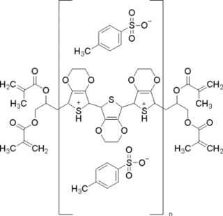
Poly(3,4-ethylenedioxythiophene)-tetramethacrylate or PEDOT-TMA is a p-type conducting polymer based on 3,4-ethylenedioxylthiophene or the EDOT monomer. It is a modification of the PEDOT structure. Advantages of this polymer relative to PEDOT are that it is dispersible in organic solvents, and it is non-corrosive. PEDOT-TMA was developed under a contract with the National Science Foundation, and it was first announced publicly on April 12, 2004. The trade name for PEDOT-TMA is Oligotron. PEDOT-TMA was featured in an article entitled "Next Stretch for Plastic Electronics" that appeared in Scientific American in 2004. The U.S. Patent office issued a patent protecting PEDOT-TMA on April 22, 2008.

Organic photovoltaic devices (OPVs) are fabricated from thin films of organic semiconductors, such as polymers and small-molecule compounds, and are typically on the order of 100 nm thick. Because polymer based OPVs can be made using a coating process such as spin coating or inkjet printing, they are an attractive option for inexpensively covering large areas as well as flexible plastic surfaces. A promising low cost alternative to conventional solar cells made of crystalline silicon, there is a large amount of research being dedicated throughout industry and academia towards developing OPVs and increasing their power conversion efficiency.

<span class="mw-page-title-main">Organic solar cell</span> Type of photovoltaic

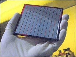
An organic solar cell (OSC) or plastic solar cell is a type of photovoltaic that uses organic electronics, a branch of electronics that deals with conductive organic polymers or small organic molecules, for light absorption and charge transport to produce electricity from sunlight by the photovoltaic effect. Most organic photovoltaic cells are polymer solar cells.

<span class="mw-page-title-main">Thin-film solar cell</span> Type of second-generation solar cell

Thin-film solar cells are made by depositing one or more thin layers of photovoltaic material onto a substrate, such as glass, plastic or metal. Thin-film solar cells are typically a few nanometers (nm) to a few microns (µm) thick–much thinner than the wafers used in conventional crystalline silicon (c-Si) based solar cells, which can be up to 200 µm thick. Thin-film solar cells are commercially used in several technologies, including cadmium telluride (CdTe), copper indium gallium diselenide (CIGS), and amorphous thin-film silicon.

<span class="mw-page-title-main">Transparent conducting film</span> Optically transparent and electrically conductive material

Transparent conducting films (TCFs) are thin films of optically transparent and electrically conductive material. They are an important component in a number of electronic devices including liquid-crystal displays, OLEDs, touchscreens and photovoltaics. While indium tin oxide (ITO) is the most widely used, alternatives include wider-spectrum transparent conductive oxides (TCOs), conductive polymers, metal grids and random metallic networks, carbon nanotubes (CNT), graphene, nanowire meshes and ultra thin metal films.

<span class="mw-page-title-main">Solar cell research</span> Research in the field of photovoltaics

There are currently many research groups active in the field of photovoltaics in universities and research institutions around the world. This research can be categorized into three areas: making current technology solar cells cheaper and/or more efficient to effectively compete with other energy sources; developing new technologies based on new solar cell architectural designs; and developing new materials to serve as more efficient energy converters from light energy into electric current or light absorbers and charge carriers.

<span class="mw-page-title-main">Nanocrystal solar cell</span>

Nanocrystal solar cells are solar cells based on a substrate with a coating of nanocrystals. The nanocrystals are typically based on silicon, CdTe or CIGS and the substrates are generally silicon or various organic conductors. Quantum dot solar cells are a variant of this approach which take advantage of quantum mechanical effects to extract further performance. Dye-sensitized solar cells are another related approach, but in this case the nano-structuring is a part of the substrate.

Thermodynamic efficiency limit is the absolute maximum theoretically possible conversion efficiency of sunlight to electricity. Its value is about 86%, which is the Chambadal-Novikov efficiency, an approximation related to the Carnot limit, based on the temperature of the photons emitted by the Sun's surface.

<span class="mw-page-title-main">Perovskite solar cell</span> Alternative to silicon-based photovoltaics

A perovskite solar cell (PSC) is a type of solar cell that includes a perovskite-structured compound, most commonly a hybrid organic–inorganic lead or tin halide-based material as the light-harvesting active layer. Perovskite materials, such as methylammonium lead halides and all-inorganic cesium lead halide, are cheap to produce and simple to manufacture.

Intermediate band photovoltaics in solar cell research provides methods for exceeding the Shockley–Queisser limit on the efficiency of a cell. It introduces an intermediate band (IB) energy level in between the valence and conduction bands. Theoretically, introducing an IB allows two photons with energy less than the bandgap to excite an electron from the valence band to the conduction band. This increases the induced photocurrent and thereby efficiency.

<span class="mw-page-title-main">Polymer-fullerene bulk heterojunction solar cell</span>

Polymer-fullerene bulk heterojunction solar cells are a type of solar cell researched in academic laboratories. Polymer-fullerene solar cells are a subset of organic solar cells, also known as organic photovoltaic (OPV) cells, which use organic materials as their active component to convert solar radiation into electrical energy. The polymer, which functions as the donor material in these solar cells, and fullerene derivatives, which function as the acceptor material, are essential components. Specifically, fullerene derivatives act as electron acceptors for donor materials like P3HT, creating a polymer-fullerene based photovoltaic cell. The Polymer-fullerene BHJ forms two channels for transferring electrons and holes to the corresponding electrodes, as opposed to the planar architecture when the Acceptor (A) and Donor (D) materials were sequentially stacked on top of each other and could selectively touch the cathode and anode electrodes. Hence, the D and A domains are expected to form a bi-continuous network with Nano-scale morphology for efficient charge transport and collection after exciton dissociation. Therefore, in the BHJ device architecture, a mixture of D and A molecules in the same or different solvents was used to form a bi-continual layer, which serves as the active layer of the device that absorbs light for exciton generation. The bi-continuous three-dimensional interpenetrating network of the BHJ design generates a greater D-A interface, which is necessary for effective exciton dissociation in the BHJ due to short exciton diffusion. When compared to the prior bilayer design, photo-generated excitons may dissociate into free holes and electrons more effectively, resulting in better charge separation for improved performance of the cell.

<span class="mw-page-title-main">Henry Snaith</span> British Professor of Physics

Henry James Snaith is a professor in physics in the Clarendon Laboratory at the University of Oxford. Research from his group has led to the creation of a new research field, based on halide perovskites for use as solar absorbers. Many individuals who were PhD students and postdoctoral researchers in Snaith's group have now established research groups, independent research portfolios and commercial enterprises. He co-founded Oxford Photovoltaics in 2010 to commercialise perovskite based tandem solar cells.

Light harvesting materials harvest solar energy that can then be converted into chemical energy through photochemical processes. Synthetic light harvesting materials are inspired by photosynthetic biological systems such as light harvesting complexes and pigments that are present in plants and some photosynthetic bacteria. The dynamic and efficient antenna complexes that are present in photosynthetic organisms has inspired the design of synthetic light harvesting materials that mimic light harvesting machinery in biological systems. Examples of synthetic light harvesting materials are dendrimers, porphyrin arrays and assemblies, organic gels, biosynthetic and synthetic peptides, organic-inorganic hybrid materials, and semiconductor materials. Synthetic and biosynthetic light harvesting materials have applications in photovoltaics, photocatalysis, and photopolymerization.

Alison Bridget Walker is a physicist who is a professor at the University of Bath. Her research considers computational modelling of printed electronic devices and the development of perovskite solar cells. She is best known for her work on the Kinetic Monte Carlo method.

References

  1. Milliron, Delia J.; Gur, Ilan; Alivisatos, A. Paul (2005). "Hybrid Organic–Nanocrystal Solar Cells". MRS Bulletin. 30: 41–44. doi:10.1557/mrs2005.8. S2CID   137370366.
  2. 1 2 Shaheen, Sean E.; Ginley, David S.; Jabbour, Ghassan E. (2005). "Organic–Based Photovoltaics". MRS Bulletin. 30: 10–19. doi: 10.1557/mrs2005.2 .
  3. 1 2 3 4 5 6 7 Saunders, B.R.; Turner, M.L. (2008). "Nanoparticle-polymer photovoltaic cells". Advances in Colloid and Interface Science. 138 (1): 1–23. doi:10.1016/j.cis.2007.09.001. PMID   17976501.
  4. Lukas, Schmidt-Mende (2016-05-24). Organic and hybrid solar cells : an introduction. Weickert, Jonas. Berlin. ISBN   9783110283204. OCLC   950902053.{{cite book}}: CS1 maint: location missing publisher (link)
  5. Sariciftci, N.S.; Smilowitz, L.; Heeger, A.J.; Wudl, F. (1993). "Semiconducting polymers (as donors) and buckminsterfullerene (as acceptor): photoinduced electron transfer and heterojunction devices". Synthetic Metals. 59 (3): 333–352. doi:10.1016/0379-6779(93)91166-Y.
  6. 1 2 3 Ginger, D.S.; Greenham, N.C. (1999). "Photoinduced electron transfer from conjugated polymers to CdSe nanocrystals". Physical Review B. 59 (16): 624–629. Bibcode:1999PhRvB..5910622G. doi:10.1103/PhysRevB.59.10622.
  7. Scheblykin, I.G.; Yartsev, A.; Pullertis, T.; Gulbinas, V.; Sundstrm, V. (2007). "Excited State and Charge Photogeneration Dynamics in Conjugated Polymers". J. Phys. Chem. B. 111 (23): 6303–6321. doi:10.1021/jp068864f. PMID   17521181.
  8. Shaw, P.E.; Ruseckas, A.; Samuel, I.D.W (2008). "Exciton Diffusion Measurements in Poly(3-hexylthiophene)". Advanced Materials. 20 (18): 3516–3520. Bibcode:2008AdM....20.3516S. doi:10.1002/adma.200800982. S2CID   136557509.
  9. A. Vats; R. Shende; J. Swiatkiewicz; J. Puszynski. "Chapter 2: Renewables: Photovoltaics, Wind & Geothermal. Mesoporous TiO2 thin-film for Dye-Sensitized Solar Cell (DSSC) Applicationv". Clean Technology 2008. Technical Proceedings of the 2008 Clean Technology Conference and Trade Show. pp. 113–116.
  10. Herman, David J.; Goldberger, Joshua E.; Chao, Stephen; Martin, Daniel T.; Stupp, Samuel I. (2011). "Orienting Periodic Organic−Inorganic Nanoscale Domains Through One-Step Electrodeposition". ACS Nano. 5 (1): 565–73. doi:10.1021/nn102697r. PMC   3127581 . PMID   21142087.
  11. Weickert, J.; Dunbar, R.B.; Wiedemann, W.; Hesse, H.C.; Schmidt-Mende, L. (2011). "Nanostructured Organic and Hybrid Solar Cells". Advanced Materials. 23 (16): 1810–28. Bibcode:2011AdM....23.1810W. doi:10.1002/adma.201003991. PMID   21509826. S2CID   16507122.
  12. Garnett, Erik C.; Brongersma, Mark L.; Cui, Yi; McGehee, Michael D. (2011). "Nanowire Solar Cells". Annual Review of Materials Research . 41: 269–295. Bibcode:2011AnRMS..41..269G. doi:10.1146/annurev-matsci-062910-100434.
  13. "Ordered Organic–Inorganic Bulk Heterojunction Photovoltaic Cells". MRS Bulletin: 37–40. 2005.
  14. 1 2 3 4 5 6 7 8 Wu, M.H; Ueda, A.; Mu, R (2005). "Semiconductor Quantum Dot Based Nanocomposite Solar Cells". Organic Photovoltaics: Mechanisms, Materials, and Devices. CRC Press. doi:10.1201/9781420026351.ch14. ISBN   978-0-8247-5963-6.
  15. 1 2 Saunders, Brian R. (March 2012). "Hybrid polymer/nanoparticle solar cells: Preparation, principles and challenges". Journal of Colloid and Interface Science. 369 (1): 1–15. Bibcode:2012JCIS..369....1S. doi:10.1016/j.jcis.2011.12.016. PMID   22209577.
  16. Dayal, Smita; Nikos Kopidakis, Dana C. Olson, David S. Ginley and Garry Rumbles; Olson, Dana C.; Ginley, David S.; Rumbles, Garry (2010). "Photovoltaic Devices with a Low Band Gap Polymer and CdSe Nanostructures Exceeding 3% Efficiency". Nano Letters. 10 (1): 239–242. Bibcode:2010NanoL..10..239D. doi:10.1021/nl903406s. PMID   20000623.{{cite journal}}: CS1 maint: multiple names: authors list (link)
  17. Charlier, J.-C.; Terrones, M.; Baxendale, M.; Meunier, V.; Zacharia, T.; Rupesinghe, N. L.; Hsu, W. K.; Grobert, N.; et al. (2002). "Enhanced Electron Field Emission in B-doped Carbon Nanotubes". Nano Letters. 2 (11): 1191–1195. Bibcode:2002NanoL...2.1191C. doi:10.1021/nl0256457.
  18. Dharap, Prasad; Li, Zhiling; Nagarajaiah, Satish; Barrera, E V (2004). "Nanotube film based on single-wall carbon nanotubes for strain sensing". Nanotechnology. 15 (3): 379–382. Bibcode:2004Nanot..15..379D. doi:10.1088/0957-4484/15/3/026. S2CID   250909198.
  19. Dekker, Cees; Tans, Sander J.; Verschueren, Alwin R. M. (1998). "Room-temperature transistor based on a single carbon nanotube". Nature. 393 (6680): 49–62. Bibcode:1998Natur.393...49T. doi:10.1038/29954. S2CID   4403144.
  20. 1 2 Cinke, Martin; Li, Jing; Chen, Bin; Cassell, Alan; Delzeit, Lance; Han, Jie; Meyyappan, M (2002). "Pore structure of raw and purified HiPco single-walled carbon nanotubes". Chemical Physics Letters. 365 (1–2): 69–74. Bibcode:2002CPL...365...69C. doi:10.1016/S0009-2614(02)01420-3. S2CID   96046204.
  21. 1 2 Somani, Prakash R.; Somani, Savita P.; Umeno, M. (2008). "Application of metal nanoparticles decorated carbon nanotubes in photovoltaics". Applied Physics Letters. 93 (3): 033315. Bibcode:2008ApPhL..93c3315S. doi:10.1063/1.2963470.
  22. 1 2 Chen, Changxin; Lu, Yang; Kong, Eric S.; Zhang, Yafei; Lee, Shuit-Tong (2008). "Nanowelded carbon-nanotube-based solar microcells". Small. 4 (9): 1313–1318. doi:10.1002/smll.200701309. PMID   18702123.
  23. 1 2 Dresselhaus, M. S. (2008). Topics in Applied Physics. Vol. 80. Springer. ISBN   978-3-540-72864-1.
  24. Collins, P. G.; Bradley, K; Ishigami, M; Zettl, A (2000). "Extreme Oxygen Sensitivity of Electronic Properties of Carbon Nanotubes". Science. 287 (5459): 1801–4. Bibcode:2000Sci...287.1801C. doi:10.1126/science.287.5459.1801. PMID   10710305.
  25. O’Regan, B. and Grätzel, M. (1991). "A low-cost, high-efficiency solar cell based on dye-sensitized colloidal TiO2 films". Nature. 353 (6346): 737–740. Bibcode:1991Natur.353..737O. doi:10.1038/353737a0. S2CID   4340159.{{cite journal}}: CS1 maint: multiple names: authors list (link)
  26. Jacques-e Moser (2005). "Solar cells: later rather than sooner". Nature Materials. 4 (10): 723–724. Bibcode:2005NatMa...4..723M. doi:10.1038/nmat1504. PMID   16195761. S2CID   1508500.
  27. Lancelle-Beltran, E.; Prené, P.; Boscher, C.; Belleville, P.; Buvat, P.; Sanchez, C. (2006). "All-Solid-State Dye-Sensitized Nanoporous TiO2 Hybrid Solar Cells with High Energy-Conversion Efficiency". Adv. Mater. 18 (19): 2579–2582. Bibcode:2006AdM....18.2579L. doi:10.1002/adma.200502023. S2CID   138764511.
  28. Sofos, Marina; Goldberger, Joshua; Stone, David A.; Allen, Jonathan E.; Ma, Qing; Herman, David J.; Tsai, Wei-Wen; Lauhon, Lincoln J.; Stupp, Samuel I. (2009). "A synergistic assembly of nanoscale lamellar photoconductor hybrids". Nature Materials. 8 (1): 68–75. Bibcode:2009NatMa...8...68S. doi:10.1038/nmat2336. PMID   19060890.