Related Research Articles
A diode is a two-terminal electronic component that conducts current primarily in one direction ; it has low resistance in one direction, and high resistance in the other. A diode vacuum tube or thermionic diode is a vacuum tube with two electrodes, a heated cathode and a plate, in which electrons can flow in only one direction, from cathode to plate. A semiconductor diode, the most commonly used type today, is a crystalline piece of semiconductor material with a p–n junction connected to two electrical terminals. Semiconductor diodes were the first semiconductor electronic devices. The discovery of asymmetric electrical conduction across the contact between a crystalline mineral and a metal was made by German physicist Ferdinand Braun in 1874. Today, most diodes are made of silicon, but other materials such as gallium arsenide and germanium are also used.

Microwaves are a form of electromagnetic radiation with wavelengths ranging from about one meter to one millimeter; with frequencies between 300 MHz (1 m) and 300 GHz (1 mm). Different sources define different frequency ranges as microwaves; the above broad definition includes both UHF and EHF bands. A more common definition in radio-frequency engineering is the range between 1 and 100 GHz. In all cases, microwaves include the entire SHF band at minimum. Frequencies in the microwave range are often referred to by their IEEE radar band designations: S, C, X, Ku, K, or Ka band, or by similar NATO or EU designations.
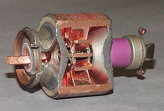
The cavity magnetron is a high-powered vacuum tube that generates microwaves using the interaction of a stream of electrons with a magnetic field while moving past a series of open metal cavities. Electrons pass by the openings to these cavities and cause microwaves to oscillate within, similar to the way a whistle produces a tone when excited by an air stream blown past its opening. The frequency of the microwaves produced, the resonant frequency, is determined by the cavities' physical dimensions. Unlike other vacuum tubes such as a klystron or a traveling-wave tube (TWT), the magnetron cannot function as an amplifier in order to increase the intensity of an applied microwave signal; the magnetron serves solely as an oscillator, generating a microwave signal from direct current electricity supplied to the vacuum tube.
A semiconductor device is an electronic component that relies on the electronic properties of a semiconductor material for its function. Semiconductor devices have replaced vacuum tubes in most applications. They use electrical conduction in the solid state rather than the gaseous state or thermionic emission in a vacuum.
A PIN diode is a diode with a wide, undoped intrinsic semiconductor region between a p-type semiconductor and an n-type semiconductor region. The p-type and n-type regions are typically heavily doped because they are used for ohmic contacts.

A bipolar junction transistor (BJT) is a type of transistor that uses both electrons and holes as charge carriers. Unipolar transistors, such as field-effect transistors, use only one kind of charge carrier. A bipolar transistor allows a small current injected at one of its terminals to control a much larger current flowing between two other terminals, making the device capable of amplification or switching.

A thyristor is a solid-state semiconductor device with four layers of alternating P- and N-type materials. It acts exclusively as a bistable switch, conducting when the gate receives a current trigger, and continuing to conduct until the voltage across the device is reversed biased, or until the voltage is removed. There are two designs, differing in what triggers the conducting state. In a three-lead thyristor, a small current on its Gate lead controls the larger current of the Anode to Cathode path. In a two-lead thyristor, conduction begins when the potential difference between the Anode and Cathode themselves is sufficiently large.

In electronics, a varicap diode, varactor diode, variable capacitance diode, variable reactance diode or tuning diode is a type of diode designed to exploit the voltage-dependent capacitance of a reverse-biased p–n junction.

A klystron is a specialized linear-beam vacuum tube, invented in 1937 by American electrical engineers Russell and Sigurd Varian, which is used as an amplifier for high radio frequencies, from UHF up into the microwave range. Low-power klystrons are used as oscillators in terrestrial microwave relay communications links, while high-power klystrons are used as output tubes in UHF television transmitters, satellite communication, radar transmitters, and to generate the drive power for modern particle accelerators.

In electronics, negative resistance (NR) is a property of some electrical circuits and devices in which an increase in voltage across the device's terminals results in a decrease in electric current through it.
In electronics, an avalanche diode is a diode that is designed to experience avalanche breakdown at a specified reverse bias voltage. The junction of an avalanche diode is designed to prevent current concentration and resulting hot spots, so that the diode is undamaged by the breakdown. The avalanche breakdown is due to minority carriers accelerated enough to create ionization in the crystal lattice, producing more carriers which in turn create more ionization. Because the avalanche breakdown is uniform across the whole junction, the breakdown voltage is nearly constant with changing current when compared to a non-avalanche diode.

An avalanche photodiode (APD) is a highly sensitive semiconductor photodiode that exploits the photoelectric effect to convert light into electricity. From a functional standpoint, they can be regarded as the semiconductor analog of photomultipliers. The avalanche photodiode (APD) was invented by Japanese engineer Jun-ichi Nishizawa in 1952. However, study of avalanche breakdown, microplasma defects in Silicon and Germanium and the investigation of optical detection using p-n junctions predate this patent. Typical applications for APDs are laser rangefinders, long-range fiber-optic telecommunication, and quantum sensing for control algorithms. New applications include positron emission tomography and particle physics. APD arrays are becoming commercially available, also lightning detection and optical SETI may be future applications.

A tunnel diode or Esaki diode is a type of semiconductor diode that has effectively "negative resistance" due to the quantum mechanical effect called tunneling. It was invented in August 1957 by Leo Esaki, Yuriko Kurose, and Takashi Suzuki when they were working at Tokyo Tsushin Kogyo, now known as Sony. In 1973, Esaki received the Nobel Prize in Physics, jointly with Brian Josephson, for discovering the electron tunneling effect used in these diodes. Robert Noyce independently devised the idea of a tunnel diode while working for William Shockley, but was discouraged from pursuing it. Tunnel diodes were first manufactured by Sony in 1957, followed by General Electric and other companies from about 1960, and are still made in low volume today.
A power semiconductor device is a semiconductor device used as a switch or rectifier in power electronics. Such a device is also called a power device or, when used in an integrated circuit, a power IC.
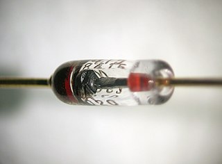
A Gunn diode, also known as a transferred electron device (TED), is a form of diode, a two-terminal semiconductor electronic component, with negative resistance, used in high-frequency electronics. It is based on the "Gunn effect" discovered in 1962 by physicist J. B. Gunn. Its largest use is in electronic oscillators to generate microwaves, in applications such as radar speed guns, microwave relay data link transmitters, and automatic door openers.
An avalanche transistor is a bipolar junction transistor designed for operation in the region of its collector-current/collector-to-emitter voltage characteristics beyond the collector-to-emitter breakdown voltage, called avalanche breakdown region. This region is characterized by avalanche breakdown, which is a phenomenon similar to Townsend discharge for gases, and negative differential resistance. Operation in the avalanche breakdown region is called avalanche-mode operation: it gives avalanche transistors the ability to switch very high currents with less than a nanosecond rise and fall times. Transistors not specifically designed for the purpose can have reasonably consistent avalanche properties; for example 82% of samples of the 15V high-speed switch 2N2369, manufactured over a 12-year period, were capable of generating avalanche breakdown pulses with rise time of 350 ps or less, using a 90V power supply as Jim Williams writes.

Avalanche breakdown is a phenomenon that can occur in both insulating and semiconducting materials. It is a form of electric current multiplication that can allow very large currents within materials which are otherwise good insulators. It is a type of electron avalanche. The avalanche process occurs when carriers in the transition region are accelerated by the electric field to energies sufficient to create mobile or free electron-hole pairs via collisions with bound electrons.

Impact ionization is the process in a material by which one energetic charge carrier can lose energy by the creation of other charge carriers. For example, in semiconductors, an electron with enough kinetic energy can knock a bound electron out of its bound state and promote it to a state in the conduction band, creating an electron-hole pair. For carriers to have sufficient kinetic energy a sufficiently large electric field must be applied, in essence requiring a sufficiently large voltage but not necessarily a large current.

The theory of solar cells explains the process by which light energy in photons is converted into electric current when the photons strike a suitable semiconductor device. The theoretical studies are of practical use because they predict the fundamental limits of a solar cell, and give guidance on the phenomena that contribute to losses and solar cell efficiency.
References
- ↑ Thomas H. Lee Planar Microwave Engineering: A Practical Guide to Theory, Measurement, and Circuits Cambridge University Press 2004 , ISBN 0521835267, pp. 296
- ↑ Sitesh Kumar Roy, Monojit Mitra, Microwave Semiconductor Devices PHI Learning Pvt. Ltd., 2003, ISBN 8120324188, page 86