A diode is a two-terminal electronic component that conducts current primarily in one direction. It has low resistance in one direction and high resistance in the other.

A transistor is a semiconductor device used to amplify or switch electrical signals and power. It is one of the basic building blocks of modern electronics. It is composed of semiconductor material, usually with at least three terminals for connection to an electronic circuit. A voltage or current applied to one pair of the transistor's terminals controls the current through another pair of terminals. Because the controlled (output) power can be higher than the controlling (input) power, a transistor can amplify a signal. Some transistors are packaged individually, but many more in miniature form are found embedded in integrated circuits. Because transistors are the key active components in practically all modern electronics, many people consider them one of the 20th century's greatest inventions.

A semiconductor device is an electronic component that relies on the electronic properties of a semiconductor material for its function. Its conductivity lies between conductors and insulators. Semiconductor devices have replaced vacuum tubes in most applications. They conduct electric current in the solid state, rather than as free electrons across a vacuum or as free electrons and ions through an ionized gas.
In physics, the term dielectric strength has the following meanings:
A bipolar junction transistor (BJT) is a type of transistor that uses both electrons and electron holes as charge carriers. In contrast, a unipolar transistor, such as a field-effect transistor (FET), uses only one kind of charge carrier. A bipolar transistor allows a small current injected at one of its terminals to control a much larger current flowing between the terminals, making the device capable of amplification or switching.

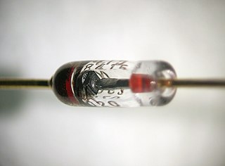
A Zener diode is a special type of diode designed to reliably allow current to flow "backwards" when a certain set reverse voltage, known as the Zener voltage, is reached.
An insulated-gate bipolar transistor (IGBT) is a three-terminal power semiconductor device primarily forming an electronic switch. It was developed to combine high efficiency with fast switching. It consists of four alternating layers (P–N–P–N) that are controlled by a metal–oxide–semiconductor (MOS) gate structure.
A thyristor is a solid-state semiconductor device with four layers of alternating P- and N-type materials used for high-power applications. It acts as a bistable switch. There are two designs, differing in what triggers the conducting state. In a three-lead thyristor, a small current on its gate lead controls the larger current of the anode-to-cathode path. In a two-lead thyristor, conduction begins when the potential difference between the anode and cathode themselves is sufficiently large. The thyristor continues conducting until the voltage across the device is reverse-biased or the voltage is removed, or through the control gate signal on newer types.
In electronics, an avalanche diode is a diode that is designed to experience avalanche breakdown at a specified reverse bias voltage. The junction of an avalanche diode is designed to prevent current concentration and resulting hot spots, so that the diode is undamaged by the breakdown. The avalanche breakdown is due to minority carriers accelerated enough to create ionization in the crystal lattice, producing more carriers, which in turn create more ionization. Because the avalanche breakdown is uniform across the whole junction, the breakdown voltage is nearly constant with changing current when compared to a non-avalanche diode.

A p–n junction is a boundary or interface between two types of semiconductor materials, p-type and n-type, inside a single crystal of semiconductor. The "p" (positive) side contains an excess of holes, while the "n" (negative) side contains an excess of electrons in the outer shells of the electrically neutral atoms there. This allows electric current to pass through the junction only in one direction. The p- and n-type regions creating the junction are made by doping the semiconductor, for example by ion implantation, diffusion of dopants, or by epitaxy.
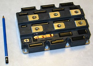
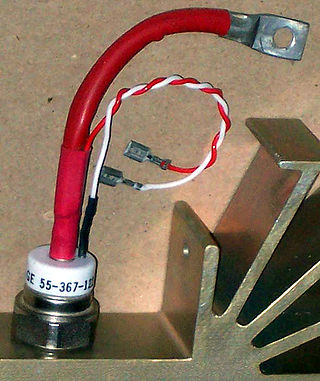
A power semiconductor device is a semiconductor device used as a switch or rectifier in power electronics. Such a device is also called a power device or, when used in an integrated circuit, a power IC.

In electronics, electrical breakdown or dielectric breakdown is a process that occurs when an electrically insulating material, subjected to a high enough voltage, suddenly becomes a conductor and current flows through it. All insulating materials undergo breakdown when the electric field caused by an applied voltage exceeds the material's dielectric strength. The voltage at which a given insulating object becomes conductive is called its breakdown voltage and, in addition to its dielectric strength, depends on its size and shape, and the location on the object at which the voltage is applied. Under sufficient voltage, electrical breakdown can occur within solids, liquids, or gases. However, the specific breakdown mechanisms are different for each kind of dielectric medium.

The breakdown voltage of an insulator is the minimum voltage that causes a portion of an insulator to experience electrical breakdown and become electrically conductive.
An IMPATT diode is a form of high-power semiconductor diode used in high-frequency microwave electronics devices. They have negative resistance and are used as oscillators and amplifiers at microwave frequencies. They operate at frequencies of about 3 and 100 GHz, or higher. The main advantage is their high-power capability; single IMPATT diodes can produce continuous microwave outputs of up to 3 kilowatts, and pulsed outputs of much higher power. These diodes are used in a variety of applications from low-power radar systems to proximity alarms. A major drawback of IMPATT diodes is the high level of phase noise they generate. This results from the statistical nature of the avalanche process.
In semiconductor physics, the depletion region, also called depletion layer, depletion zone, junction region, space charge region, or space charge layer, is an insulating region within a conductive, doped semiconductor material where the mobile charge carriers have diffused away, or forced away by an electric field. The only elements left in the depletion region are ionized donor or acceptor impurities. This region of uncovered positive and negative ions is called the depletion region due to the depletion of carriers in this region, leaving none to carry a current. Understanding the depletion region is key to explaining modern semiconductor electronics: diodes, bipolar junction transistors, field-effect transistors, and variable capacitance diodes all rely on depletion region phenomena.

Impact ionization is the process in a material by which one energetic charge carrier can lose energy by the creation of other charge carriers. For example, in semiconductors, an electron with enough kinetic energy can knock a bound electron out of its bound state and promote it to a state in the conduction band, creating an electron-hole pair. For carriers to have sufficient kinetic energy a sufficiently large electric field must be applied, in essence requiring a sufficiently large voltage but not necessarily a large current.
Hot carrier injection (HCI) is a phenomenon in solid-state electronic devices where an electron or a “hole” gains sufficient kinetic energy to overcome a potential barrier necessary to break an interface state. The term "hot" refers to the effective temperature used to model carrier density, not to the overall temperature of the device. Since the charge carriers can become trapped in the gate dielectric of a MOS transistor, the switching characteristics of the transistor can be permanently changed. Hot-carrier injection is one of the mechanisms that adversely affects the reliability of semiconductors of solid-state devices.
In electronics, leakage is the gradual transfer of electrical energy across a boundary normally viewed as insulating, such as the spontaneous discharge of a charged capacitor, magnetic coupling of a transformer with other components, or flow of current across a transistor in the "off" state or a reverse-polarized diode.

In electronics, the Zener effect is a type of electrical breakdown, discovered by Clarence Melvin Zener. It occurs in a reverse biased p-n diode when the electric field enables tunneling of electrons from the valence to the conduction band of a semiconductor, leading to numerous free minority carriers which suddenly increase the reverse current.
This article provides a more detailed explanation of p–n diode behavior than is found in the articles p–n junction or diode.
