Breakdown voltage

Last updated
High voltage breakdown of an insulator string Lfa.JPG
High voltage breakdown of an insulator string

The breakdown voltage of an insulator is the minimum voltage that causes a portion of an insulator to experience electrical breakdown and become electrically conductive.

Contents

For diodes, the breakdown voltage is the minimum reverse voltage that makes the diode conduct appreciably in reverse. Some devices (such as TRIACs) also have a forward breakdown voltage.

Electrical breakdown

Materials are often classified as conductors or insulators based on their resistivity. A conductor is a substance which contains many mobile charged particles called charge carriers which are free to move about inside the material. An electric field is created across a piece of the material by applying a voltage difference between electrical contacts on different sides of the material. The force of the field causes the charge carriers within the material to move, creating an electric current from the positive contact to the negative contact. For example, in metals one or more of the negatively charged electrons in each atom, called conduction electrons, are free to move about the crystal lattice. An electric field causes a large current to flow, so metals have low resistivity, making them good conductors. In contrast in materials like plastics and ceramics all the electrons are tightly bound to atoms, so under normal conditions there are very few mobile charge carriers in the material. Applying a voltage causes only a very small current to flow, giving the material a very high resistivity, and these are classed as insulators.

However, if a strong enough electric field is applied, all insulators become conductors. If the voltage applied across a piece of insulator is increased, at a certain electric field strength the number of charge carriers in the material suddenly increases enormously and its resistivity drops, causing a strong current to flow through it. This is called electrical breakdown. Breakdown occurs when the electric field becomes strong enough to pull electrons from the molecules of the material, ionizing them. The released electrons are accelerated by the field and strike other atoms, creating more free electrons and ions in a chain reaction, flooding the material with charged particles. This occurs at a characteristic electric field strength in each material, measured in volts per centimeter, called its dielectric strength.

When a voltage is applied across a piece of insulator, the electric field at each point is equal to the gradient of the voltage. The voltage gradient may vary at different points across the object, due to its shape or local variations in composition. Electrical breakdown occurs when the field first exceeds the dielectric strength of the material in some region of the object. Once one area has broken down and become conductive, that area has almost no voltage drop and the full voltage is applied across the remaining length of the insulator, resulting in a higher gradient and electric field, causing additional areas in the insulator to break down. The breakdown quickly spreads in a conductive path through the insulator until it extends from the positive to the negative contact. The voltage at which this occurs is called the breakdown voltage of that object. Breakdown voltage [1] varies with the material composition, shape of an object, and the length of material between the electrical contacts.

Solids

Breakdown voltage is a characteristic of an insulator that defines the maximum voltage difference that can be applied across the material before the insulator conducts. In solid insulating materials, this usually[ citation needed ] creates a weakened path within the material by creating permanent molecular or physical changes by the sudden current. Within rarefied gases found in certain types of lamps, breakdown voltage is also sometimes called the striking voltage. [2]

The breakdown voltage of a material is not a definite value because it is a form of failure and there is a statistical probability whether the material will fail at a given voltage. When a value is given it is usually the mean breakdown voltage of a large sample. Another term is withstand voltage , where the probability of failure at a given voltage is so low it is considered, when designing insulation, that the material will not fail at this voltage.

Two different breakdown voltage measurements of a material are the AC and impulse breakdown voltages. The AC voltage is the line frequency of the mains. The impulse breakdown voltage is simulating lightning strikes, and usually uses a 1.2 microsecond rise for the wave to reach 90% amplitude, then drops back down to 50% amplitude after 50 microseconds. [3]

Two technical standards governing performing these tests are ASTM D1816 and ASTM D3300 published by ASTM. [4]

Gases and vacuum

In standard conditions at atmospheric pressure, air serves as an excellent insulator, requiring the application of a significant voltage of 3.0 kV/mm before breaking down (e.g., lightning, or sparking across plates of a capacitor, or the electrodes of a spark plug). Using other gases, this breakdown potential may decrease to an extent that two uninsulated surfaces with different potentials might induce the electrical breakdown of the surrounding gas. This may damage an apparatus, as a breakdown is analogous to a short circuit.

In a gas, the breakdown voltage can be determined by Paschen's law.

The breakdown voltage in a partial vacuum is represented as [5] [6] [7]

where is the breakdown potential in volts DC, and are constants that depend on the surrounding gas, represents the pressure of the surrounding gas, represents the distance in centimetres between the electrodes,[ clarification needed ] and represents the Secondary Electron Emission Coefficient.

A detailed derivation, and some background information, is given in the article about Paschen's law.

Diodes and other semiconductors

Diode I-V diagram Diode-IV-Curve.svg
Diode I-V diagram

Breakdown voltage is a parameter of a diode that defines the largest reverse voltage that can be applied without causing an exponential increase in the leakage current in the diode. Exceeding the breakdown voltage of a diode, per se, is not destructive; although, exceeding its current capacity will be. In fact, Zener diodes are essentially just heavily doped normal diodes that exploit the breakdown voltage of a diode to provide regulation of voltage levels.

Rectifier diodes (semiconductor or tube/valve) may have several voltage ratings, such as the peak inverse voltage (PIV) across the diode, and the maximum RMS input voltage to the rectifier circuit (which will be much less).

Many small-signal transistors need to have any breakdown currents limited to much lower values to avoid excessive heating. To avoid damage to the device, and to limit the effects excessive leakage current may have on the surrounding circuit, the following bipolar transistor maximum ratings are often specified:

VCEO (sometimes written BVCEO or V(BR)CEO)
The maximum voltage between collector and emitter that can be safely applied (and with no more than some specified leakage current, often) when no circuit at the base of the transistor is there to remove collector-base leakage. Typical values: 20 volts to as high as 700 volts; very early Germanium point-contact transistors such as the OC10 had values around 5 volts or less.
VCBO
The maximum collector-to-base voltage, with emitter open-circuit. Typical values 25 to 1200 volts.
VCER
The maximum voltage rating between collector and emitter with some specified resistance (or less) between base and emitter. A more realistic rating for real-world circuits than the open-base or open-emitter scenarios above.
VEBO
The maximum reverse voltage on the base with respect to the emitter. Typically around 5 volts - more for germanium transistors, less for UHF transistors usually.
VCES
Collector to emitter rating when base is shorted to emitter; equivalent to VCER when R = 0.
VCEX
Collector to emitter rating when a specific base-emitter voltage is supplied, such as in some high voltage switching scenarios.

Field-effect transistors have similar maximum ratings, the most important one for junction FETs is the gate-drain voltage rating.

Some devices may also have a maximum rate of change of voltage specified.

Electrical apparatus

Power transformers, circuit breakers, switchgear and other electrical apparatus connected to overhead transmission lines are exposed to transient lightning surge voltages induced on the power circuit. Electrical apparatus will have a basic lightning impulse level (BIL) specified. This is the crest value of an impulse waveform with a standardized wave shape, intended to simulate the electrical stress of a lightning surge or a surge induced by circuit switching. The BIL is coordinated with the typical operating voltage of the apparatus. For high-voltage transmission lines, the impulse level is related to the clearance to ground of energized components. As an example, a transmission line rated 138 kV would be designed for a BIL of 650 kV. A higher BIL may be specified than the minimum, where the exposure to lightning is severe. [8]

See also

Related Research Articles

<span class="mw-page-title-main">Electric current</span> Flow of electric charge

An electric current is a flow of charged particles, such as electrons or ions, moving through an electrical conductor or space. It is defined as the net rate of flow of electric charge through a surface. The moving particles are called charge carriers, which may be one of several types of particles, depending on the conductor. In electric circuits the charge carriers are often electrons moving through a wire. In semiconductors they can be electrons or holes. In an electrolyte the charge carriers are ions, while in plasma, an ionized gas, they are ions and electrons.

<span class="mw-page-title-main">Diode</span> Two-terminal electronic component

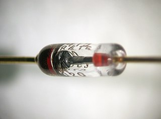
A diode is a two-terminal electronic component that conducts current primarily in one direction. It has low resistance in one direction and high resistance in the other.

<span class="mw-page-title-main">Insulator (electricity)</span> Material that does not conduct an electric current

An electrical insulator is a material in which electric current does not flow freely. The atoms of the insulator have tightly bound electrons which cannot readily move. Other materials—semiconductors and conductors—conduct electric current more easily. The property that distinguishes an insulator is its resistivity; insulators have higher resistivity than semiconductors or conductors. The most common examples are non-metals.

<span class="mw-page-title-main">Multivibrator</span> Electronic circuit used to implement two-state devices

A multivibrator is an electronic circuit used to implement a variety of simple two-state devices such as relaxation oscillators, timers, latches and flip-flops. The first multivibrator circuit, the astable multivibrator oscillator, was invented by Henri Abraham and Eugene Bloch during World War I. It consisted of two vacuum tube amplifiers cross-coupled by a resistor-capacitor network. They called their circuit a "multivibrator" because its output waveform was rich in harmonics. A variety of active devices can be used to implement multivibrators that produce similar harmonic-rich wave forms; these include transistors, neon lamps, tunnel diodes and others. Although cross-coupled devices are a common form, single-element multivibrator oscillators are also common.

<span class="mw-page-title-main">Transistor</span> Solid-state electrically operated switch also used as an amplifier

A transistor is a semiconductor device used to amplify or switch electrical signals and power. It is one of the basic building blocks of modern electronics. It is composed of semiconductor material, usually with at least three terminals for connection to an electronic circuit. A voltage or current applied to one pair of the transistor's terminals controls the current through another pair of terminals. Because the controlled (output) power can be higher than the controlling (input) power, a transistor can amplify a signal. Some transistors are packaged individually, but many more in miniature form are found embedded in integrated circuits. Because transistors are the key active components in practically all modern electronics, many people consider them one of the 20th century's greatest inventions.

<span class="mw-page-title-main">Vacuum tube</span> Device that controls current between electrodes

A vacuum tube, electron tube, valve, or tube, is a device that controls electric current flow in a high vacuum between electrodes to which an electric potential difference has been applied.

<span class="mw-page-title-main">MOSFET</span> Type of field-effect transistor

The metal–oxide–semiconductor field-effect transistor is a type of field-effect transistor (FET), most commonly fabricated by the controlled oxidation of silicon. It has an insulated gate, the voltage of which determines the conductivity of the device. This ability to change conductivity with the amount of applied voltage can be used for amplifying or switching electronic signals. The term metal–insulator–semiconductor field-effect transistor (MISFET) is almost synonymous with MOSFET. Another near-synonym is insulated-gate field-effect transistor (IGFET).

In physics, the term dielectric strength has the following meanings:

<span class="mw-page-title-main">Bipolar junction transistor</span> Transistor that uses both electrons and holes as charge carriers

A bipolar junction transistor (BJT) is a type of transistor that uses both electrons and electron holes as charge carriers. In contrast, a unipolar transistor, such as a field-effect transistor (FET), uses only one kind of charge carrier. A bipolar transistor allows a small current injected at one of its terminals to control a much larger current flowing between the terminals, making the device capable of amplification or switching.

<span class="mw-page-title-main">Zener diode</span> Diode that allows current to flow in the reverse direction at a specific voltage

A Zener diode is a special type of diode designed to reliably allow current to flow "backwards" when a certain set reverse voltage, known as the Zener voltage, is reached.

In electronics, an avalanche diode is a diode that is designed to experience avalanche breakdown at a specified reverse bias voltage. The junction of an avalanche diode is designed to prevent current concentration and resulting hot spots, so that the diode is undamaged by the breakdown. The avalanche breakdown is due to minority carriers accelerated enough to create ionization in the crystal lattice, producing more carriers, which in turn create more ionization. Because the avalanche breakdown is uniform across the whole junction, the breakdown voltage is nearly constant with changing current when compared to a non-avalanche diode.

<span class="mw-page-title-main">Spark gap</span> Two conducting electrodes separated in order to allow an electric spark to pass between

A spark gap consists of an arrangement of two conducting electrodes separated by a gap usually filled with a gas such as air, designed to allow an electric spark to pass between the conductors. When the potential difference between the conductors exceeds the breakdown voltage of the gas within the gap, a spark forms, ionizing the gas and drastically reducing its electrical resistance. An electric current then flows until the path of ionized gas is broken or the current reduces below a minimum value called the "holding current". This usually happens when the voltage drops, but in some cases occurs when the heated gas rises, stretching out and then breaking the filament of ionized gas. Usually, the action of ionizing the gas is violent and disruptive, often leading to sound, light, and heat.

p–n junction Semiconductor–semiconductor junction

A p–n junction is a boundary or interface between two types of semiconductor materials, p-type and n-type, inside a single crystal of semiconductor. The "p" (positive) side contains an excess of holes, while the "n" (negative) side contains an excess of electrons in the outer shells of the electrically neutral atoms there. This allows electric current to pass through the junction only in one direction. The p- and n-type regions creating the junction are made by doping the semiconductor, for example by ion implantation, diffusion of dopants, or by epitaxy.

<span class="mw-page-title-main">Electrical breakdown</span> Conduction of electricity through an insulator under sufficiently high voltage

In electronics, electrical breakdown or dielectric breakdown is a process that occurs when an electrically insulating material, subjected to a high enough voltage, suddenly becomes a conductor and current flows through it. All insulating materials undergo breakdown when the electric field caused by an applied voltage exceeds the material's dielectric strength. The voltage at which a given insulating object becomes conductive is called its breakdown voltage and, in addition to its dielectric strength, depends on its size and shape, and the location on the object at which the voltage is applied. Under sufficient voltage, electrical breakdown can occur within solids, liquids, or gases. However, the specific breakdown mechanisms are different for each kind of dielectric medium.

<span class="mw-page-title-main">Marx generator</span> High-voltage pulse generator

A Marx generator is an electrical circuit first described by Erwin Otto Marx in 1924. Its purpose is to generate a high-voltage pulse from a low-voltage DC supply. Marx generators are used in high-energy physics experiments, as well as to simulate the effects of lightning on power-line gear and aviation equipment. A bank of 36 Marx generators is used by Sandia National Laboratories to generate X-rays in their Z Machine.

<span class="mw-page-title-main">High voltage</span> Electrical potential which is large enough to cause damage or injury

High voltage electricity refers to electrical potential large enough to cause injury or damage. In certain industries, high voltage refers to voltage above a certain threshold. Equipment and conductors that carry high voltage warrant special safety requirements and procedures.

<span class="mw-page-title-main">Capacitor</span> Passive two-terminal electronic component that stores electrical energy in an electric field

In electrical engineering, a capacitor is a device that stores electrical energy by accumulating electric charges on two closely spaced surfaces that are insulated from each other. The capacitor was originally known as the condenser, a term still encountered in a few compound names, such as the condenser microphone. It is a passive electronic component with two terminals.

<span class="mw-page-title-main">LED circuit</span> Electrical circuit used to power a LED

In electronics, an LED circuit or LED driver is an electrical circuit used to power a light-emitting diode (LED). The circuit must provide sufficient current to light the LED at the required brightness, but must limit the current to prevent damaging the LED. The voltage drop across an LED is approximately constant over a wide range of operating current; therefore, a small increase in applied voltage greatly increases the current. Very simple circuits are used for low-power indicator LEDs. More complex, current source circuits are required when driving high-power LEDs for illumination to achieve correct current regulation.

In electronics, leakage is the gradual transfer of electrical energy across a boundary normally viewed as insulating, such as the spontaneous discharge of a charged capacitor, magnetic coupling of a transformer with other components, or flow of current across a transistor in the "off" state or a reverse-polarized diode.

<span class="mw-page-title-main">Noise generator</span> Circuit that produces electrical noise

A noise generator is a circuit that produces electrical noise. Noise generators are used to test signals for measuring noise figure, frequency response, and other parameters. Noise generators are also used for generating random numbers.

References

  1. "Benefits of BDV testing?". www.pact.in.
  2. J. M. Meek and J. D. Craggs, Electrical Breakdown of Gases, John Wiley & Sons, Chichester, 1978.
  3. Emelyanov, A.A., Izv. Vyssh. Uchebn. Zaved., Fiz., 1989, no. 4, p. 103.
  4. Kalyatskii, I.I., Kassirov, G.M., and Smirnov, G.V., Prib. Tekh. Eksp., 1974, no. 4, p. 84.
  5. G. Cuttone, C. Marchetta, L. Torrisi, G. Della Mea, A. Quaranta, V. Rigato and S. Zandolin, Surface Treatment of HV Electrodes for Superconducting Cyclotron Beam Extraction, IEEE. Trans. DEI, Vol. 4, pp. 218<223, 1997.
  6. H. Moscicka-Grzesiak, H. Gruszka and M. Stroinski, ‘‘Influence of Electrode Curvature on Predischarge Phenomena and Electric Strength at 50 Hz of a Vacuum
  7. R. V. Latham, High Voltage Vacuum Insulation: Basic concepts and technological practice, Academic Press, London, 1995.
  8. D. G. Fink, H. W. Beaty, Standard Handbook for Electrical Engineers, Eleventh Edition, McGraw-Hill, 1978, ISBN   007020974X, page 17-20 ff