Very Large Scale Integration

Last updated

Very-large-scale integration (VLSI) is the process of creating an integrated circuit (IC) by combining millions or billions of MOS transistors onto a single chip. VLSI began in the 1970s when MOS integrated circuit (Metal Oxide Semiconductor) chips were developed and then widely adopted, enabling complex semiconductor and telecommunication technologies. The microprocessor and memory chips are VLSI devices.

Contents

Before the introduction of VLSI technology, most ICs had a limited set of functions they could perform. An electronic circuit might consist of a CPU, ROM, RAM and other glue logic. VLSI enables IC designers to add all of these into one chip.

A VLSI integrated-circuit die Diopsis.jpg
A VLSI integrated-circuit die

History

Background

The history of the transistor dates to the 1920s when several inventors attempted devices that were intended to control current in solid-state diodes and convert them into triodes. Success came after World War II, when the use of silicon and germanium crystals as radar detectors led to improvements in fabrication and theory. Scientists who had worked on radar returned to solid-state device development. With the invention of the first transistor at Bell Labs in 1947, the field of electronics shifted from vacuum tubes to solid-state devices.

With the small transistor at their hands, electrical engineers of the 1950s saw the possibilities of constructing far more advanced circuits. However, as the complexity of circuits grew, problems arose. [1] One problem was the size of the circuit. A complex circuit like a computer was dependent on speed. If the components were large, the wires interconnecting them must be long. The electric signals took time to go through the circuit, thus slowing the computer. [1]

The invention of the integrated circuit by Jack Kilby and Robert Noyce solved this problem by making all the components and the chip out of the same block (monolith) of semiconductor material. The circuits could be made smaller, and the manufacturing process could be automated. This led to the idea of integrating all components on a single-crystal silicon wafer, which led to small-scale integration (SSI) in the early 1960s, and then medium-scale integration (MSI) in the late 1960s.

VLSI

General Microelectronics introduced the first commercial MOS integrated circuit in 1964. [2] In the early 1970s, MOS integrated circuit technology allowed the integration of more than 10,000 transistors in a single chip. [3] This paved the way for VLSI in the 1970s and 1980s, with tens of thousands of MOS transistors on a single chip (later hundreds of thousands, then millions, and now billions).

The first semiconductor chips held two transistors each. Subsequent advances added more transistors, and as a consequence, more individual functions or systems were integrated over time. The first integrated circuits held only a few devices, perhaps as many as ten diodes, transistors, resistors and capacitors, making it possible to fabricate one or more logic gates on a single device. Now known retrospectively as small-scale integration (SSI), improvements in technique led to devices with hundreds of logic gates, known as medium-scale integration (MSI). Further improvements led to large-scale integration (LSI), i.e. systems with at least a thousand logic gates. Current technology has moved far past this mark and today's microprocessors have many millions of gates and billions of individual transistors.

At one time, there was an effort to name and calibrate various levels of large-scale integration above VLSI. Terms like ultra-large-scale integration (ULSI) were used. But the huge number of gates and transistors available on common devices has rendered such fine distinctions moot. Terms suggesting greater than VLSI levels of integration are no longer in widespread use.

In 2008, billion-transistor processors became commercially available. This became more commonplace as semiconductor fabrication advanced from the then-current generation of 65 nm processors. Current designs, unlike the earliest devices, use extensive design automation and automated logic synthesis to lay out the transistors, enabling higher levels of complexity in the resulting logic functionality. Certain high-performance logic blocks like the SRAM (static random-access memory) cell, are still designed by hand to ensure the highest efficiency.[ citation needed ]

Structured design

Structured VLSI design is a modular methodology originated by Carver Mead and Lynn Conway for saving microchip area by minimizing the interconnect fabric area. This is obtained by repetitive arrangement of rectangular macro blocks which can be interconnected using wiring by abutment. An example is partitioning the layout of an adder into a row of equal bit slices cells. In complex designs this structuring may be achieved by hierarchical nesting. [4]

Structured VLSI design had been popular in the early 1980s, but lost its popularity later[ citation needed ] because of the advent of placement and routing tools wasting a lot of area by routing, which is tolerated because of the progress of Moore's Law. When introducing the hardware description language KARL in the mid-1970s, Reiner Hartenstein coined the term "structured VLSI design" (originally as "structured LSI design"), echoing Edsger Dijkstra's structured programming approach by procedure nesting to avoid chaotic spaghetti-structured programs.

Difficulties

As microprocessors become more complex due to technology scaling, microprocessor designers have encountered several challenges which force them to think beyond the design plane, and look ahead to post-silicon:

See also

Related Research Articles

Processor design is a subfield of computer science and computer engineering (fabrication) that deals with creating a processor, a key component of computer hardware.

<span class="mw-page-title-main">Integrated circuit</span> Electronic circuit formed on a small, flat piece of semiconductor material

An integrated circuit is a set of electronic circuits on one small flat piece of semiconductor material, usually silicon. In an IC, a large numbers of miniaturized transistors and other electronic components are integrated together on the chip. This results in circuits that are orders of magnitude smaller, faster, and less expensive than those constructed of discrete components, allowing a large transistor count.

<span class="mw-page-title-main">Semiconductor device fabrication</span> Manufacturing process used to create integrated circuits

Semiconductor device fabrication is the process used to manufacture semiconductor devices, typically integrated circuits (ICs) such as computer processors, microcontrollers, and memory chips that are present in everyday electrical and electronic devices. It is a multiple-step photolithographic and physio-chemical process during which electronic circuits are gradually created on a wafer, typically made of pure single-crystal semiconducting material. Silicon is almost always used, but various compound semiconductors are used for specialized applications.

<span class="mw-page-title-main">MOSFET</span> Type of field-effect transistor

The metal–oxide–semiconductor field-effect transistor is a type of field-effect transistor (FET), most commonly fabricated by the controlled oxidation of silicon. It has an insulated gate, the voltage of which determines the conductivity of the device. This ability to change conductivity with the amount of applied voltage can be used for amplifying or switching electronic signals. The term metal–insulator–semiconductor field-effect transistor (MISFET) is almost synonymous with MOSFET. Another near-synonym is insulated-gate field-effect transistor (IGFET).

<span class="mw-page-title-main">CMOS</span> Technology for constructing integrated circuits

Complementary metal–oxide–semiconductor is a type of metal–oxide–semiconductor field-effect transistor (MOSFET) fabrication process that uses complementary and symmetrical pairs of p-type and n-type MOSFETs for logic functions. CMOS technology is used for constructing integrated circuit (IC) chips, including microprocessors, microcontrollers, memory chips, and other digital logic circuits. CMOS technology is also used for analog circuits such as image sensors, data converters, RF circuits, and highly integrated transceivers for many types of communication.

<span class="mw-page-title-main">Intel 4004</span> 4-bit microprocessor

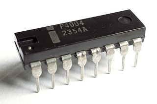
The Intel 4004 is a 4-bit central processing unit (CPU) released by Intel Corporation in 1971. Sold for US$60, it was the first commercially produced microprocessor, and the first in a long line of Intel CPUs.

<span class="mw-page-title-main">Application-specific integrated circuit</span> Integrated circuit customized for a specific task

An application-specific integrated circuit is an integrated circuit (IC) chip customized for a particular use, rather than intended for general-purpose use, such as a chip designed to run in a digital voice recorder or a high-efficiency video codec. Application-specific standard product chips are intermediate between ASICs and industry standard integrated circuits like the 7400 series or the 4000 series. ASIC chips are typically fabricated using metal–oxide–semiconductor (MOS) technology, as MOS integrated circuit chips.

Bipolar CMOS (BiCMOS) is a semiconductor technology that integrates two semiconductor technologies, those of the bipolar junction transistor and the CMOS logic gate, into a single integrated circuit. In more recent times the bipolar processes have been extended to include high mobility devices using silicon–germanium junctions.

In computer engineering, a logic family is one of two related concepts:

<span class="mw-page-title-main">Miniaturization</span> Trend to manufacture ever smaller products and devices

Miniaturization is the trend to manufacture ever-smaller mechanical, optical, and electronic products and devices. Examples include miniaturization of mobile phones, computers and vehicle engine downsizing. In electronics, the exponential scaling and miniaturization of silicon MOSFETs leads to the number of transistors on an integrated circuit chip doubling every two years, an observation known as Moore's law. This leads to MOS integrated circuits such as microprocessors and memory chips being built with increasing transistor density, faster performance, and lower power consumption, enabling the miniaturization of electronic devices.

<span class="mw-page-title-main">Mixed-signal integrated circuit</span> Integrated circuit

A mixed-signal integrated circuit is any integrated circuit that has both analog circuits and digital circuits on a single semiconductor die. Their usage has grown dramatically with the increased use of cell phones, telecommunications, portable electronics, and automobiles with electronics and digital sensors.

<span class="mw-page-title-main">Depletion-load NMOS logic</span> Form of digital logic family in integrated circuits

In integrated circuits, depletion-load NMOS is a form of digital logic family that uses only a single power supply voltage, unlike earlier NMOS logic families that needed more than one different power supply voltage. Although manufacturing these integrated circuits required additional processing steps, improved switching speed and the elimination of the extra power supply made this logic family the preferred choice for many microprocessors and other logic elements.

<span class="mw-page-title-main">Integrated circuit design</span> Engineering process for electronic hardware

Integrated circuit design, or IC design, is a sub-field of electronics engineering, encompassing the particular logic and circuit design techniques required to design integrated circuits, or ICs. ICs consist of miniaturized electronic components built into an electrical network on a monolithic semiconductor substrate by photolithography.

In semiconductor electronics fabrication technology, a self-aligned gate is a transistor manufacturing approach whereby the gate electrode of a MOSFET is used as a mask for the doping of the source and drain regions. This technique ensures that the gate is naturally and precisely aligned to the edges of the source and drain.

Four-phase logic is a type of, and design methodology for dynamic logic. It enabled non-specialist engineers to design quite complex ICs, using either PMOS or NMOS processes. It uses a kind of 4-phase clock signal.

<span class="mw-page-title-main">PMOS logic</span> Family of digital circuits

PMOS or pMOS logic is a family of digital circuits based on p-channel, enhancement mode metal–oxide–semiconductor field-effect transistors (MOSFETs). In the late 1960s and early 1970s, PMOS logic was the dominant semiconductor technology for large-scale integrated circuits before being superseded by NMOS and CMOS devices.

A three-dimensional integrated circuit is a MOS integrated circuit (IC) manufactured by stacking as many as 16 or more ICs and interconnecting them vertically using, for instance, through-silicon vias (TSVs) or Cu-Cu connections, so that they behave as a single device to achieve performance improvements at reduced power and smaller footprint than conventional two dimensional processes. The 3D IC is one of several 3D integration schemes that exploit the z-direction to achieve electrical performance benefits in microelectronics and nanoelectronics.

In semiconductor manufacturing, a process corner is an example of a design-of-experiments (DoE) technique that refers to a variation of fabrication parameters used in applying an integrated circuit design to a semiconductor wafer. Process corners represent the extremes of these parameter variations within which a circuit that has been etched onto the wafer must function correctly. A circuit running on devices fabricated at these process corners may run slower or faster than specified and at lower or higher temperatures and voltages, but if the circuit does not function at all at any of these process extremes the design is considered to have inadequate design margin.

Glossary of microelectronics manufacturing terms

References

  1. 1 2 "The History of the Integrated Circuit". Nobelprize.org. Archived from the original on 29 Jun 2018. Retrieved 21 Apr 2012.
  2. "1964: First Commercial MOS IC Introduced". Computer History Museum .
  3. Hittinger, William C. (1973). "Metal-Oxide-Semiconductor Technology". Scientific American. 229 (2): 48–59. Bibcode:1973SciAm.229b..48H. doi:10.1038/scientificamerican0873-48. ISSN   0036-8733. JSTOR   24923169.
  4. Jain, B. K. (August 2009). Digital Electronics - A Modern Approach by B K Jain. ISBN   9788182202153 . Retrieved 2 May 2017.

Further reading