TO-92

Last updated
TO-92 Front with Pin Numbers.svg
TO-92 front view [1]
TO-92 Back with Pin Numbers.svg
TO-92 back view [1]

The TO-92 is a widely used style of semiconductor package mainly used for transistors. The case is often made of epoxy or plastic, and offers compact size at a very low cost.

Contents

History and origin

The JEDEC TO-92 descriptor is derived from the original full name for the package: Transistor Outline Package, Case Style 92. [1] The package is also known by the designation SOT54. By 1966 the package was being used by Motorola for their 2N3904 devices among others. [2]
Construction and orientation

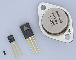
Size comparison of BJT transistor packages, from left to right: SOT-23, TO-92, TO-126, TO-3 Transistorer (cropped).jpg
Size comparison of BJT transistor packages, from left to right: SOT-23, TO-92, TO-126, TO-3

The case is molded around the transistor elements in two parts; the face is flat, usually bearing a machine-printed part number (some early examples had the part number printed on the top surface instead). The back is semi-circularly-shaped. A line of moulding flash from the injection-moulding process can be seen around the case.

The leads protrude from the bottom of the case. When looking at the face of the transistor, the leads are commonly configured from left-to-right as the emitter, base, and collector for 2N series (JEDEC) transistors, however, other configurations are possible, such as emitter, collector, and base commonly used for 2S series (Japanese) transistors or collector, base, and emitter for many of the BC series (Pro Electron) types.

If the face has a part name made up of only one letter and a few numbers, it can be either a Japanese or a Pro Electron part number. Thus, "C1234" would likely be a 2SC1234 device, but "C547" is usually short for "BC547".

TO-92 packages with pre-bent wires; on the left to emulate a TO-18 footprint (SO-97 in BS 3934, 10A3 in DIN 41868) To-92 footprint.jpg
TO-92 packages with pre-bent wires; on the left to emulate a TO-18 footprint (SO-97 in BS 3934, 10A3 in DIN 41868)

The leads coming out of the case are spaced 0.05" (1.27 mm) apart. It is often convenient to bend them outward to a 0.10" (2.54 mm) spacing to make more room for wiring. [3] Units with their leads pre-bent may be ordered to fit specific board layouts, depending on the application. Otherwise, the leads may be bent manually; however, care must be taken as they can break easily, as with any other device that is manually configured.

The physical dimensions of the TO-92 housing may vary slightly depending on the manufacturer, however, the 1.27mm lead spacing must be respected.

Advantages

Disadvantages

The main disadvantage of this style of case is the lack of heat sinking.

Voltage and current

Although TO-92 devices are mainly used in low-voltage / low-current (<30 V; <1 A) applications, high-voltage (600 Volt Vce) and high-current (5 A Ic) devices are available. Nominal maximum power dissipation is less than one watt (600 mW).

Variants

For diodes or integrated circuits with two connections (e.g. temperature sensors) the middle lead is either not connected or omitted entirely.

Comparison between the E-Line/Miniplast package and the TO-92 package Miniplast vs TO-92.jpg
Comparison between the E-Line/Miniplast package and the TO-92 package

In the late 1960s, Ferranti introduced a smaller package with a compatible footprint, called "E-Line". [4] [5] This package was later standardized as a British Standard (but not by JEDEC) and remained in production with Ferranti Semiconductors' successor companies (Plessey, Zetex Semiconductors, Diodes Incorporated [6] ). In East Germany the E-Line package was known as the "Miniplast" package and widely used by Kombinat Mikroelektronik Erfurt.

Standards

Standards organizationStandardDesignation for
TO-92E-Line/Miniplast
3-lead2-lead
IEC IEC 60191 [7] A68
DIN DIN 41868 [8] 10B3 [lower-alpha 1]
EIAJ / JEITA ED-7500A [9] [10] SC-43A
British Standards BS 3934 [11] SO-94 [lower-alpha 2]
Gosstandart GOST 18472—88 [12] KT-26 [lower-alpha 3] KD-129 [lower-alpha 4]
Rosstandart GOST R 57439—2017 [13]
Kombinat Mikroelektronik Erfurt TGL 200-8380 [14] L2
TGL 11811 [7] L3
TGL 26713/07 [7] F2F3F4
  1. DIN 41868 also defines variants with the leads bent to emulate the footprint of other packages: 10A3 (TO-18 footprint).
  2. BS-3934 also defines variants with the leads bent to emulate the footprint of other packages: SO-95 (TO-5 footprint), SO-96 (for flat mounting), and SO-97 (TO-18 footprint).
  3. Russian: КТ-26
  4. Russian: КД-129

Common components in a TO-92 package

Common transistors:

Other common components:

Related Research Articles

<span class="mw-page-title-main">Transistor</span> Solid-state electrically operated switch also used as an amplifier

A transistor is a semiconductor device used to amplify or switch electrical signals and power. It is one of the basic building blocks of modern electronics. It is composed of semiconductor material, usually with at least three terminals for connection to an electronic circuit. A voltage or current applied to one pair of the transistor's terminals controls the current through another pair of terminals. Because the controlled (output) power can be higher than the controlling (input) power, a transistor can amplify a signal. Some transistors are packaged individually, but many more in miniature form are found embedded in integrated circuits. Because transistors are the key active components in practically all modern electronics, many people consider them one of the 20th century's greatest inventions.

Pro Electron or EECA is the European type designation and registration system for active components.

<span class="mw-page-title-main">TO-220</span> Power semiconductor through-hole package

The TO-220 is a style of electronic package used for high-powered, through-hole components with 0.1 inches (2.54 mm) pin spacing. The "TO" designation stands for "transistor outline". TO-220 packages have three leads. Similar packages with two, four, five or seven leads are also manufactured. A notable characteristic is a metal tab with a hole, used to mount the case to a heatsink, allowing the component to dissipate more heat than one constructed in a TO-92 case. Common TO-220-packaged components include discrete semiconductors such as transistors and silicon-controlled rectifiers, as well as integrated circuits.

<span class="mw-page-title-main">2N3055</span> Early power transistor

The 2N3055 is a silicon NPN power transistor intended for general purpose applications. It was introduced in the early 1960s by RCA using a hometaxial power transistor process, transitioned to an epitaxial base in the mid-1970s. Its numbering follows the JEDEC standard. It is a transistor type of enduring popularity.

<span class="mw-page-title-main">TO-3</span> Metal can semiconductor package for power semiconductors

In electronics, TO-3 is a designation for a standardized metal semiconductor package used for power semiconductors, including transistors, silicon controlled rectifiers, and, integrated circuits. TO stands for "Transistor Outline" and relates to a series of technical drawings produced by JEDEC.

<span class="mw-page-title-main">2N3904</span> Common NPN bipolar junction transistor

The 2N3904 is a common NPN bipolar junction transistor used for general-purpose low-power amplifying or switching applications. It is designed for low current and power, medium voltage, and can operate at moderately high speeds. It is complementary to the 2N3906 PNP transistor. Both types were registered by Motorola Semiconductor in the mid-1960s.

<span class="mw-page-title-main">2N2222</span> Common NPN bipolar junction transistor

The 2N2222 is a common NPN bipolar junction transistor (BJT) used for general purpose low-power amplifying or switching applications. It is designed for low to medium current, low power, medium voltage, and can operate at moderately high speeds. It was originally made in the TO-18 metal can as shown in the picture.

The 2N2907 is a commonly available PNP bipolar junction transistor used for general purpose low-power amplifying or switching applications. It is designed for low to medium current, low power, medium voltage, and can operate at moderately high speeds. This transistor was made by several manufacturers; Texas Instruments released a data sheet for their version of this part dated March 1973. An "A" suffix indicates a slightly higher breakdown voltage. These transistors have an enduring popularity with electronics hobbyists.

<span class="mw-page-title-main">2N3906</span> Common PNP bipolar junction transistor

The 2N3906 is a commonly used PNP bipolar junction transistor intended for general purpose low-power amplifying or switching applications. It is designed for low electric current and power and medium voltage, and can operate at moderately high speeds. It is complementary to the 2N3904 NPN transistor. Both types were registered by Motorola Semiconductor in the mid-1960s.

<span class="mw-page-title-main">1N4148 signal diode</span> Standard silicon switching diode

The 1N4148 is a standard silicon switching signal diode. It is one of the most popular and long-lived switching diodes because of its dependable specifications and low cost. Its name follows the JEDEC nomenclature. The 1N4148 is useful in switching applications up to about 100 MHz with a reverse-recovery time of no more than 4 ns.

<span class="mw-page-title-main">BC548</span>

The BC548 is a general-purpose NPN bipolar junction transistor commonly used in European and American electronic equipment. It is notably often the first type of bipolar transistor hobbyists encounter and is often featured in designs in hobby electronics magazines where a general-purpose transistor is required. The BC548 is low in cost and widely available.

A semiconductor package is a metal, plastic, glass, or ceramic casing containing one or more discrete semiconductor devices or integrated circuits. Individual components are fabricated on semiconductor wafers before being diced into die, tested, and packaged. The package provides a means for connecting it to the external environment, such as printed circuit board, via leads such as lands, balls, or pins; and protection against threats such as mechanical impact, chemical contamination, and light exposure. Additionally, it helps dissipate heat produced by the device, with or without the aid of a heat spreader. There are thousands of package types in use. Some are defined by international, national, or industry standards, while others are particular to an individual manufacturer.

<span class="mw-page-title-main">TO-18</span>

In electronics, TO-18 is a designation for a style of transistor metal case. The case is more expensive than the similarly sized plastic TO-92 package. The name is from JEDEC, signifying Transistor Outline Package, Case Style 18.

<span class="mw-page-title-main">DO-204</span>

DO-204 is a family of diode semiconductor packages defined by JEDEC. This family comprises lead-mounted axial devices with round leads. Generally a diode will have a line painted near the cathode end.

<span class="mw-page-title-main">Small-outline transistor</span> Family of discrete surface mount transistors

A small outline transistor (SOT) is a family of small footprint, discrete surface mount transistor commonly used in consumer electronics. The most common SOT are SOT23 variations,. SOT23-5 differs from SOT23 in a wider body of 1.6 mm (0.063 in) instead of 1.3 mm (0.051 in). Also, manufacturers offer the nearly identical thin small outline transistor (TSOT/TSOP) package, where lower height is important.

<span class="mw-page-title-main">TO-5</span> Standardized metal semiconductor package

In electronics, TO-5 is a designation for a standardized metal semiconductor package used for transistors and some integrated circuits. The TO element stands for "transistor outline" and refers to a series of technical drawings produced by JEDEC. The first commercial silicon transistors, the 2N696 and 2N697 from Fairchild Semiconductor, came in a TO-5 package.

<span class="mw-page-title-main">TO-126</span>

TO-126 is a type of semiconductor package for devices with three pins, such as transistors. The package is rectangular with a hole in the middle to allow for easy mounting to a board or a heat sink. On one side of the package typically a metal sheet is exposed, with the transistor die bonded to the other side of the metal sheet inside the package. This allows for an efficient heat transfer from the transistor die to an external heat sink but also implies that the metal sheet is electrically connected to the die.

<span class="mw-page-title-main">TO-66</span> Smaller variant of the TO-3 package

TO-66 is a type of semiconductor package for devices with three connections, such as transistors. The shape is similar to the TO-3 package, but the size is smaller. The TO-66 package is made entirely of metal and is commonly used by silicon controlled rectifiers and power transistors. In Europe, it was popularly used by the complementary germanium power transistors AD161/AD162.

<span class="mw-page-title-main">TO-8</span>

In electronics, TO-8 is a designation for a standardized metal semiconductor package. TO in TO-8 stands for "transistor outline" and refers to a series of technical drawings produced by JEDEC. The TO-8 package is noticeably larger than the more common TO-5 package. While originally designed for medium power transistors such as the 2N1483 series or the AD136, it is more commonly used for integrated circuits and sensors.

References

  1. 1 2 3 "JEDEC TO-92 package specification" (PDF). JEDEC . Archived from the original (PDF) on June 18, 2017.
  2. The semiconductor data book. Motorola. August 1966. Retrieved 2021-07-09.
  3. Bourns. "Package Mechanical Information, TO-92" (PDF). Retrieved 28 February 2016.
  4. Applications of the E-Line Plastic Encapsulated Transistor. Oldham: Ferranti Ltd. June 1969. Retrieved 2021-07-10.
  5. "E-Line – The ultimate TO-92". Quick Reference Guide (PDF). Ferranti Semiconductors. February 1983. p. E2. Retrieved 2021-07-10.
  6. "E-Line Package Information" (PDF). Diodes Incorporated. March 2017. Retrieved 2021-07-10.
  7. 1 2 3 "TGL 26713/07: Gehäuse für Halbleiterbauelemente - Bauform F" [Outline drawings for semiconductor devices; Type F](PDF) (in German). Leipzig: Verlag für Standardisierung. June 1988. Retrieved 2021-06-15.
  8. "Semiconductor Databook" (PDF). Heilbronn: AEG-Telefunken. pp. 17, 19. Retrieved 2021-08-20.
  9. "EIAJ ED-7500A Standards for the Dimensions of Semiconductor Devices" (PDF). JEITA. 1996. p. 120. Retrieved 2021-06-14.
  10. "TO-92 (SOT54)". Nexperia. 2004-11-16. Archived from the original on 2017-12-13. Retrieved 2021-07-12.
  11. "Package Outlines". Quick Reference Guide (PDF). Ferranti Semiconductors. February 1983. p. PO14. Retrieved 2021-07-10.
  12. "ГОСТ 18472—88 ПРИБОРЫ ПОЛУПРОВОДНИКОВЫЕ - Основные размеры" [GOST 18472—88 Semiconductor devices - basic dimensions](PDF) (in Russian). Rosstandart. 1988. p. 33-34,55. Retrieved 2021-06-17.
  13. "ГОСТ Р 57439—2017 ПРИБОРЫ ПОЛУПРОВОДНИКОВЫЕ - Основные размеры" [GOST R 57439—2017 Semiconductor devices - basic dimensions](PDF) (in Russian). Gosstandart. 2017. p. 41-42,68-69. Retrieved 2021-06-17.
  14. "TGL 200-8380: Halbleiterbauelemente - Halbleiterdioden Verlustleistung unter 1 Watt - Bauformen" [Semiconductor Devices - Designs for Semiconductor Diodes - Dissipation power less 1 Watt](PDF) (in German). Leipzig: Verlag für Standardisierung. 1981. Retrieved 2021-07-12.