
A transistor is a semiconductor device used to amplify or switch electrical signals and power. It is one of the basic building blocks of modern electronics. It is composed of semiconductor material, usually with at least three terminals for connection to an electronic circuit. A voltage or current applied to one pair of the transistor's terminals controls the current through another pair of terminals. Because the controlled (output) power can be higher than the controlling (input) power, a transistor can amplify a signal. Some transistors are packaged individually, but many more in miniature form are found embedded in integrated circuits. Because transistors are the key active components in practically all modern electronics, many people consider them one of the 20th century's greatest inventions.

A semiconductor device is an electronic component that relies on the electronic properties of a semiconductor material for its function. Its conductivity lies between conductors and insulators. Semiconductor devices have replaced vacuum tubes in most applications. They conduct electric current in the solid state, rather than as free electrons across a vacuum or as free electrons and ions through an ionized gas.

The metal–oxide–semiconductor field-effect transistor is a type of field-effect transistor (FET), most commonly fabricated by the controlled oxidation of silicon. It has an insulated gate, the voltage of which determines the conductivity of the device. This ability to change conductivity with the amount of applied voltage can be used for amplifying or switching electronic signals. The term metal–insulator–semiconductor field-effect transistor (MISFET) is almost synonymous with MOSFET. Another near-synonym is insulated-gate field-effect transistor (IGFET).

In microelectronics, a dual in-line package is an electronic component package with a rectangular housing and two parallel rows of electrical connecting pins. The package may be through-hole mounted to a printed circuit board (PCB) or inserted in a socket. The dual-inline format was invented by Don Forbes, Rex Rice and Bryant Rogers at Fairchild R&D in 1964, when the restricted number of leads available on circular transistor-style packages became a limitation in the use of integrated circuits. Increasingly complex circuits required more signal and power supply leads ; eventually microprocessors and similar complex devices required more leads than could be put on a DIP package, leading to development of higher-density chip carriers. Furthermore, square and rectangular packages made it easier to route printed-circuit traces beneath the packages.

Surface-mount technology (SMT), originally called planar mounting, is a method in which the electrical components are mounted directly onto the surface of a printed circuit board (PCB). An electrical component mounted in this manner is referred to as a surface-mount device (SMD). In industry, this approach has largely replaced the through-hole technology construction method of fitting components, in large part because SMT allows for increased manufacturing automation which reduces cost and improves quality. It also allows for more components to fit on a given area of substrate. Both technologies can be used on the same board, with the through-hole technology often used for components not suitable for surface mounting such as large transformers and heat-sinked power semiconductors.

The zig-zag in-line package (ZIP) is a packaging technology for integrated circuits. It was intended as a replacement for dual in-line packaging. A ZIP is an integrated circuit encapsulated in a slab of plastic with 16, 20, 28 or 40 pins, measuring about 3 mm x 30 mm x 10 mm. The package's pins protrude in two rows from one of the long edges. The two rows are staggered by 1.27 mm (0.05"), giving them a zig-zag appearance, and allowing them to be spaced more closely than a rectangular grid would allow. The pins are inserted into holes in a printed circuit board, with the packages standing at right-angles to the board, allowing them to be placed closer together than DIPs of the same size. ZIPs have now been superseded by surface-mount packages such as the thin small-outline packages (TSOPs), but are still in use. The quad in-line package uses a similar staggered semiconductor package design.

The 7400 series is a popular logic family of transistor–transistor logic (TTL) integrated circuits (ICs).

The 555 timer IC is an integrated circuit used in a variety of timer, delay, pulse generation, and oscillator applications. It is one of the most popular timing ICs due to its flexibility and price. Derivatives provide two or four timing circuits in one package. The design was first marketed in 1972 by Signetics and used bipolar junction transistors. Since then, numerous companies have made the original timers and later similar low-power CMOS timers. In 2017, it was said that over a billion 555 timers are produced annually by some estimates, and that the design was "probably the most popular integrated circuit ever made".

In electronics, through-hole technology is a manufacturing scheme in which leads on the components are inserted through holes drilled in printed circuit boards (PCB) and soldered to pads on the opposite side, either by manual assembly or by the use of automated insertion mount machines.

A small outline integrated circuit (SOIC) is a surface-mounted integrated circuit (IC) package which occupies an area about 30–50% less than an equivalent dual in-line package (DIP), with a typical thickness being 70% less. They are generally available in the same pin-outs as their counterpart DIP ICs. The convention for naming the package is SOIC or SO followed by the number of pins. For example, a 14-pin 4011 would be housed in an SOIC-14 or SO-14 package.
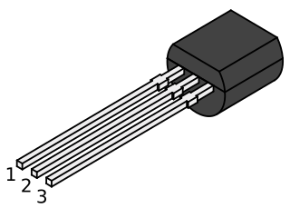
The TO-92 is a widely used style of semiconductor package mainly used for transistors. The case is often made of epoxy or plastic, and offers compact size at a very low cost.

The TO-220 is a style of electronic package used for high-powered, through-hole components with 0.1 inches (2.54 mm) pin spacing. The "TO" designation stands for "transistor outline". TO-220 packages have three leads. Similar packages with two, four, five or seven leads are also manufactured. A notable characteristic is a metal tab with a hole, used to mount the case to a heatsink, allowing the component to dissipate more heat than one constructed in a TO-92 case. Common TO-220-packaged components include discrete semiconductors such as transistors and silicon-controlled rectifiers, as well as integrated circuits.
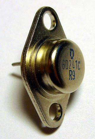
In electronics, TO-3 is a designation for a standardized metal semiconductor package used for power semiconductors, including transistors, silicon controlled rectifiers, and, integrated circuits. TO stands for "Transistor Outline" and relates to a series of technical drawings produced by JEDEC.
A transistor is a semiconductor device with at least three terminals for connection to an electric circuit. In the common case, the third terminal controls the flow of current between the other two terminals. This can be used for amplification, as in the case of a radio receiver, or for rapid switching, as in the case of digital circuits. The transistor replaced the vacuum-tube triode, also called a (thermionic) valve, which was much larger in size and used significantly more power to operate. The first transistor was successfully demonstrated on December 23, 1947, at Bell Laboratories in Murray Hill, New Jersey. Bell Labs was the research arm of American Telephone and Telegraph (AT&T). The three individuals credited with the invention of the transistor were William Shockley, John Bardeen and Walter Brattain. The introduction of the transistor is often considered one of the most important inventions in history.

Metal electrode leadless face (MELF) is a type of leadless cylindrical electronic surface mount device that is metallized at its ends. MELF devices are usually diodes and resistors.

78xx is a family of self-contained fixed linear voltage regulator integrated circuits. The 78xx family is commonly used in electronic circuits requiring a regulated power supply due to their ease-of-use and low cost.

In electronics, a chip carrier is one of several kinds of surface-mount technology packages for integrated circuits. Connections are made on all four edges of a square package; compared to the internal cavity for mounting the integrated circuit, the package overall size is large.
TO-66 is a type of semiconductor package for devices with three connections, such as transistors. The shape is similar to the TO-3 package, but the size is smaller. The TO-66 package is made entirely of metal and is commonly used by silicon controlled rectifiers and power transistors. In Europe, it was popularly used by the complementary germanium power transistors AD161/AD162.

TO-252, also known as DPAK or Decawatt Package, is a semiconductor package developed by Motorola for surface mounting on circuit boards. It represents a surface-mount variant of TO-251 package, and smaller variant of the D2PAK package. It is often used for high-power MOSFETs and voltage regulators.


 A pair of MOSFETs in the surface-mount package D2PAK.
 A TO-220 package compared to a D2PAK package.

