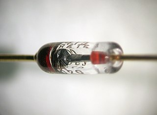
A diode is a two-terminal electronic component that conducts current primarily in one direction. It has low resistance in one direction and high resistance in the other.
A semiconductor is a material that has an electrical conductivity value falling between that of a conductor, such as copper, and an insulator, such as glass. Its resistivity generally falls as its temperature rises; metals behave in the opposite way. In many cases their conducting properties may be altered in useful ways by introducing impurities ("doping") into the crystal structure. When two differently doped regions exist in the same crystal, a semiconductor junction is created. The behavior of charge carriers, which include electrons, ions, and electron holes, at these junctions is the basis of diodes, transistors, and most modern electronics. Some examples of semiconductors are silicon, germanium, gallium arsenide, and elements near the so-called "metalloid staircase" on the periodic table. After silicon, gallium arsenide is the second-most common semiconductor and is used in laser diodes, solar cells, microwave-frequency integrated circuits, and others. Silicon is a critical element for fabricating most electronic circuits.

A transistor is a semiconductor device used to amplify or switch electrical signals and power. It is one of the basic building blocks of modern electronics. It is composed of semiconductor material, usually with at least three terminals for connection to an electronic circuit. A voltage or current applied to one pair of the transistor's terminals controls the current through another pair of terminals. Because the controlled (output) power can be higher than the controlling (input) power, a transistor can amplify a signal. Some transistors are packaged individually, but many more in miniature form are found embedded in integrated circuits. Because transistors are the key active components in practically all modern electronics, many people consider them one of the 20th century's greatest inventions.

A semiconductor device is an electronic component that relies on the electronic properties of a semiconductor material for its function. Its conductivity lies between conductors and insulators. Semiconductor devices have replaced vacuum tubes in most applications. They conduct electric current in the solid state, rather than as free electrons across a vacuum or as free electrons and ions through an ionized gas.

The metal–oxide–semiconductor field-effect transistor is a type of field-effect transistor (FET), most commonly fabricated by the controlled oxidation of silicon. It has an insulated gate, the voltage of which determines the conductivity of the device. This ability to change conductivity with the amount of applied voltage can be used for amplifying or switching electronic signals. The term metal–insulator–semiconductor field-effect transistor (MISFET) is almost synonymous with MOSFET. Another near-synonym is insulated-gate field-effect transistor (IGFET).
A bipolar junction transistor (BJT) is a type of transistor that uses both electrons and electron holes as charge carriers. In contrast, a unipolar transistor, such as a field-effect transistor (FET), uses only one kind of charge carrier. A bipolar transistor allows a small current injected at one of its terminals to control a much larger current flowing between the terminals, making the device capable of amplification or switching.

Gallium arsenide (GaAs) is a III-V direct band gap semiconductor with a zinc blende crystal structure.

A p–n junction is a boundary or interface between two types of semiconductor materials, p-type and n-type, inside a single crystal of semiconductor. The "p" (positive) side contains an excess of holes, while the "n" (negative) side contains an excess of electrons in the outer shells of the electrically neutral atoms there. This allows electric current to pass through the junction only in one direction. The p- and n-type regions creating the junction are made by doping the semiconductor, for example by ion implantation, diffusion of dopants, or by epitaxy.

A high-electron-mobility transistor, also known as heterostructure FET (HFET) or modulation-doped FET (MODFET), is a field-effect transistor incorporating a junction between two materials with different band gaps as the channel instead of a doped region. A commonly used material combination is GaAs with AlGaAs, though there is wide variation, dependent on the application of the device. Devices incorporating more indium generally show better high-frequency performance, while in recent years, gallium nitride HEMTs have attracted attention due to their high-power performance. Like other FETs, HEMTs are used in integrated circuits as digital on-off switches. FETs can also be used as amplifiers for large amounts of current using a small voltage as a control signal. Both of these uses are made possible by the FET’s unique current–voltage characteristics. HEMT transistors are able to operate at higher frequencies than ordinary transistors, up to millimeter wave frequencies, and are used in high-frequency products such as cell phones, satellite television receivers, voltage converters, and radar equipment. They are widely used in satellite receivers, in low power amplifiers and in the defense industry.

In semiconductor production, doping is the intentional introduction of impurities into an intrinsic (undoped) semiconductor for the purpose of modulating its electrical, optical and structural properties. The doped material is referred to as an extrinsic semiconductor.

The point-contact transistor was the first type of transistor to be successfully demonstrated. It was developed by research scientists John Bardeen and Walter Brattain at Bell Laboratories in December 1947. They worked in a group led by physicist William Shockley. The group had been working together on experiments and theories of electric field effects in solid state materials, with the aim of replacing vacuum tubes with a smaller device that consumed less power.
In semiconductor electronics fabrication technology, a self-aligned gate is a transistor manufacturing approach whereby the gate electrode of a MOSFET is used as a mask for the doping of the source and drain regions. This technique ensures that the gate is naturally and precisely aligned to the edges of the source and drain.
An extrinsic semiconductor is one that has been doped; during manufacture of the semiconductor crystal a trace element or chemical called a doping agent has been incorporated chemically into the crystal, for the purpose of giving it different electrical properties than the pure semiconductor crystal, which is called an intrinsic semiconductor. In an extrinsic semiconductor it is these foreign dopant atoms in the crystal lattice that mainly provide the charge carriers which carry electric current through the crystal. The doping agents used are of two types, resulting in two types of extrinsic semiconductor. An electron donor dopant is an atom which, when incorporated in the crystal, releases a mobile conduction electron into the crystal lattice. An extrinsic semiconductor that has been doped with electron donor atoms is called an n-type semiconductor, because the majority of charge carriers in the crystal are negative electrons. An electron acceptor dopant is an atom which accepts an electron from the lattice, creating a vacancy where an electron should be called a hole which can move through the crystal like a positively charged particle. An extrinsic semiconductor which has been doped with electron acceptor atoms is called a p-type semiconductor, because the majority of charge carriers in the crystal are positive holes.

The germanium alloy-junction transistor, or alloy transistor, was an early type of bipolar junction transistor, developed at General Electric and RCA in 1951 as an improvement over the earlier grown-junction transistor.
A diffused junction transistor is a transistor formed by diffusing dopants into a semiconductor substrate. The diffusion process was developed later than the alloy-junction and grown junction processes for making bipolar junction transistors (BJTs).
A transistor is a semiconductor device with at least three terminals for connection to an electric circuit. In the common case, the third terminal controls the flow of current between the other two terminals. This can be used for amplification, as in the case of a radio receiver, or for rapid switching, as in the case of digital circuits. The transistor replaced the vacuum-tube triode, also called a (thermionic) valve, which was much larger in size and used significantly more power to operate. The first transistor was successfully demonstrated on December 23, 1947, at Bell Laboratories in Murray Hill, New Jersey. Bell Labs was the research arm of American Telephone and Telegraph (AT&T). The three individuals credited with the invention of the transistor were William Shockley, John Bardeen and Walter Brattain. The introduction of the transistor is often considered one of the most important inventions in history.
Monocrystalline silicon, more often called single-crystal silicon, in short mono c-Si or mono-Si, is the base material for silicon-based discrete components and integrated circuits used in virtually all modern electronic equipment. Mono-Si also serves as a photovoltaic, light-absorbing material in the manufacture of solar cells.
The first planar monolithic integrated circuit (IC) chip was demonstrated in 1960. The idea of integrating electronic circuits into a single device was born when the German physicist and engineer Werner Jacobi developed and patented the first known integrated transistor amplifier in 1949 and the British radio engineer Geoffrey Dummer proposed to integrate a variety of standard electronic components in a monolithic semiconductor crystal in 1952. A year later, Harwick Johnson filed a patent for a prototype IC. Between 1953 and 1957, Sidney Darlington and Yasuo Tarui proposed similar chip designs where several transistors could share a common active area, but there was no electrical isolation to separate them from each other.

The field-effect transistor (FET) is a type of transistor that uses an electric field to control the flow of current in a semiconductor. It comes in two types: junction FET (JFET) and metal-oxide-semiconductor FET (MOSFET). FETs have three terminals: source, gate, and drain. FETs control the flow of current by the application of a voltage to the gate, which in turn alters the conductivity between the drain and source.
Morris Tanenbaum was an American physical chemist and executive who worked at Bell Laboratories and AT&T Corporation.
