
An operational amplifier is a DC-coupled high-gain electronic voltage amplifier with a differential input and, usually, a single-ended output. In this configuration, an op amp produces an output potential that is typically 100,000 times larger than the potential difference between its input terminals. The operational amplifier traces its origin and name to analog computers, where they were used to perform mathematical operations in linear, non-linear, and frequency-dependent circuits.

A transistor is a semiconductor device used to amplify or switch electrical signals and power. It is one of the basic building blocks of modern electronics. It is composed of semiconductor material, usually with at least three terminals for connection to an electronic circuit. A voltage or current applied to one pair of the transistor's terminals controls the current through another pair of terminals. Because the controlled (output) power can be higher than the controlling (input) power, a transistor can amplify a signal. Some transistors are packaged individually, but many more in miniature form are found embedded in integrated circuits. Because transistors are the key active components in practically all modern electronics, many people consider them one of the 20th century's greatest inventions.

In electronics, a comparator is a device that compares two voltages or currents and outputs a digital signal indicating which is larger. It has two analog input terminals and and one binary digital output . The output is ideally
Transistor–transistor logic (TTL) is a logic family built from bipolar junction transistors. Its name signifies that transistors perform both the logic function and the amplifying function, as opposed to earlier resistor–transistor logic (RTL) and diode–transistor logic (DTL).
A bipolar junction transistor (BJT) is a type of transistor that uses both electrons and electron holes as charge carriers. In contrast, a unipolar transistor, such as a field-effect transistor (FET), uses only one kind of charge carrier. A bipolar transistor allows a small current injected at one of its terminals to control a much larger current flowing between the terminals, making the device capable of amplification or switching.
N-type metal–oxide–semiconductor logic uses n-type (-) MOSFETs to implement logic gates and other digital circuits. These nMOS transistors operate by creating an inversion layer in a p-type transistor body. This inversion layer, called the n-channel, can conduct electrons between n-type "source" and "drain" terminals. The n-channel is created by applying voltage to the third terminal, called the gate. Like other MOSFETs, nMOS transistors have four modes of operation: cut-off, triode, saturation, and velocity saturation.

In digital logic, an inverter or NOT gate is a logic gate which implements logical negation. It outputs a bit opposite of the bit that is put into it. The bits are typically implemented as two differing voltage levels.
In electronics, a multi-transistor configuration called the Darlington configuration is a circuit consisting of two bipolar transistors with the emitter of one transistor connected to the base of the other, such that the current amplified by the first transistor is amplified further by the second one. The collectors of both transistors are connected together. This configuration has a much higher current gain than each transistor taken separately. It acts like and is often packaged as a single transistor. It was invented in 1953 by Sidney Darlington.
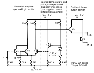
In electronics, emitter-coupled logic (ECL) is a high-speed integrated circuit bipolar transistor logic family. ECL uses an overdriven bipolar junction transistor (BJT) differential amplifier with single-ended input and limited emitter current to avoid the saturated region of operation and its slow turn-off behavior. As the current is steered between two legs of an emitter-coupled pair, ECL is sometimes called current-steering logic (CSL), current-mode logic (CML) or current-switch emitter-follower (CSEF) logic.

A differential amplifier is a type of electronic amplifier that amplifies the difference between two input voltages but suppresses any voltage common to the two inputs. It is an analog circuit with two inputs and and one output , in which the output is ideally proportional to the difference between the two voltages:

In electronics, a Schmitt trigger is a comparator circuit with hysteresis implemented by applying positive feedback to the noninverting input of a comparator or differential amplifier. It is an active circuit which converts an analog input signal to a digital output signal. The circuit is named a trigger because the output retains its value until the input changes sufficiently to trigger a change. In the non-inverting configuration, when the input is higher than a chosen threshold, the output is high. When the input is below a different (lower) chosen threshold the output is low, and when the input is between the two levels the output retains its value. This dual threshold action is called hysteresis and implies that the Schmitt trigger possesses memory and can act as a bistable multivibrator. There is a close relation between the two kinds of circuits: a Schmitt trigger can be converted into a latch and a latch can be converted into a Schmitt trigger.
Resistor–transistor logic (RTL), sometimes also known as transistor–resistor logic (TRL), is a class of digital circuits built using resistors as the input network and bipolar junction transistors (BJTs) as switching devices. RTL is the earliest class of transistorized digital logic circuit; it was succeeded by diode–transistor logic (DTL) and transistor–transistor logic (TTL).

Diode–transistor logic (DTL) is a class of digital circuits that is the direct ancestor of transistor–transistor logic. It is called so because the logic gating functions AND and OR are performed by diode logic, while logical inversion (NOT) and amplification is performed by a transistor.

A buffer amplifier is one that provides electrical impedance transformation from one circuit to another, with the aim of preventing the signal source from being affected by whatever currents that the load may impose. The signal is 'buffered from' load currents. Two main types of buffer exist: the voltage buffer and the current buffer.

In electronics, a common-emitter amplifier is one of three basic single-stage bipolar-junction-transistor (BJT) amplifier topologies, typically used as a voltage amplifier. It offers high current gain, medium input resistance and a high output resistance. The output of a common emitter amplifier is 180 degrees out of phase to the input signal.
In computer engineering, a logic family is one of two related concepts:

IC power-supply pins denote a voltage and current supply terminals in electric, electronics engineering, and in Integrated circuit design. Integrated circuits (ICs) have at least two pins that connect to the power rails of the circuit in which they are installed. These are known as the power-supply pins. However, the labeling of the pins varies by IC family and manufacturer. The double subscript notation usually corresponds to a first letter in a given IC family (transistors) notation of the terminals.
Diode logic constructs AND and OR logic gates with diodes and resistors.
Open collector output and open drain output utilize a transistor as a switch that either disconnects or connects an integrated circuit (IC) output pin to ground, instead of outputting a specific voltage or current.

The diamond buffer or diamond follower is a four-transistor, two-stage, push-pull, translinear emitter follower, or less commonly source follower, in which the input transistors are folded, or placed upside-down with respect to the output transistors. Like any unity buffer, the diamond buffer does not alter the phase and magnitude of input voltage signal; its primary purpose is to interface a high-impedance voltage source with a low-impedance, high-current load. Unlike the more common compound emitter follower, where each input transistor drives the output transistor of the same polarity, each input transistor of a diamond buffer drives the output transistor of the opposite polarity. When the transistors operate in close thermal contact, the input transistors stabilize the idle current of the output pair, eliminating the need for a bias spreader.


