Related Research Articles

A logic gate is a device that performs a Boolean function, a logical operation performed on one or more binary inputs that produces a single binary output. Depending on the context, the term may refer to an ideal logic gate, one that has, for instance, zero rise time and unlimited fan-out, or it may refer to a non-ideal physical device.
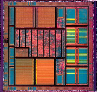
Very-large-scale integration (VLSI) is the process of creating an integrated circuit (IC) by combining millions or billions of MOS transistors onto a single chip. VLSI began in the 1970s when MOS integrated circuit chips were developed and then widely adopted, enabling complex semiconductor and telecommunication technologies. The microprocessor and memory chips are VLSI devices.
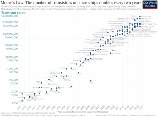
Moore's law is the observation that the number of transistors in an integrated circuit (IC) doubles about every two years. Moore's law is an observation and projection of a historical trend. Rather than a law of physics, it is an empirical relationship linked to gains from experience in production.

Complementary metal–oxide–semiconductor is a type of metal–oxide–semiconductor field-effect transistor (MOSFET) fabrication process that uses complementary and symmetrical pairs of p-type and n-type MOSFETs for logic functions. CMOS technology is used for constructing integrated circuit (IC) chips, including microprocessors, microcontrollers, memory chips, and other digital logic circuits. CMOS technology is also used for analog circuits such as image sensors, data converters, RF circuits, and highly integrated transceivers for many types of communication.

EEPROM or E2PROM (electrically erasable programmable read-only memory) is a type of non-volatile memory. It is used in computers, usually integrated in microcontrollers such as smart cards and remote keyless systems, or as a separate chip device, to store relatively small amounts of data by allowing individual bytes to be erased and reprogrammed.

In integrated circuits, depletion-load NMOS is a form of digital logic family that uses only a single power supply voltage, unlike earlier NMOS logic families that needed more than one different power supply voltage. Although manufacturing these integrated circuits required additional processing steps, improved switching speed and the elimination of the extra power supply made this logic family the preferred choice for many microprocessors and other logic elements.

Integrated injection logic (IIL, I2L, or I2L) is a class of digital circuits built with multiple collector bipolar junction transistors (BJT). When introduced it had speed comparable to TTL yet was almost as low power as CMOS, making it ideal for use in VLSI (and larger) integrated circuits. The gates can be made smaller with this logic family than with CMOS because complementary transistors are not needed. Although the logic voltage levels are very close (High: 0.7V, Low: 0.2V), I2L has high noise immunity because it operates by current instead of voltage. I2L was developed in 1971 by Siegfried K. Wiedmann and Horst H. Berger who originally called it merged-transistor logic (MTL). A disadvantage of this logic family is that the gates draw power when not switching unlike with CMOS.
The transistor count is the number of transistors in an electronic device. It is the most common measure of integrated circuit complexity. The rate at which MOS transistor counts have increased generally follows Moore's law, which observes that transistor count doubles approximately every two years. However, being directly proportional to the area of a die, transistor count does not represent how advanced the corresponding manufacturing technology is. A better indication of this is transistor density which is the ratio of a semiconductor's transistor count to its die area.
SONOS, short for "silicon–oxide–nitride–oxide–silicon", more precisely, "polycrystalline silicon"—"silicon dioxide"—"silicon nitride"—"silicon dioxide"—"silicon", is a cross sectional structure of MOSFET (metal–oxide–semiconductor field-effect transistor), realized by P.C.Y. Chen of Fairchild Camera and Instrument in 1977. This structure is often used for non-volatile memories, such as EEPROM and flash memories. It is sometimes used for TFT LCD displays. It is one of CTF (charge trap flash) variants. It is distinguished from traditional non-volatile memory structures by the use of silicon nitride (Si3N4 or Si9N10) instead of "polysilicon-based FG (floating-gate)" for the charge storage material. A further variant is "SHINOS" ("silicon"—"hi-k"—"nitride"—"oxide"—"silicon"), which is substituted top oxide layer with high-κ material. Another advanced variant is "MONOS" ("metal–oxide–nitride–oxide–silicon"). Companies offering SONOS-based products include Cypress Semiconductor, Macronix, Toshiba, United Microelectronics Corporation and Floadia.

Domino logic is a CMOS-based evolution of dynamic logic techniques consisting of a dynamic logic gate cascaded into a static CMOS inverter. The term derives from the fact that in domino logic, each stage ripples the next stage for evaluation, similar to dominoes falling one after the other. Domino logic contrasts with other solutions to the cascade problem where cascading is interrupted by clocks or other means.
This is the history of the transistor. A transistor is a semiconductor device with at least three terminals for connection to an electric circuit. In the common case, the third terminal controls the flow of current between the other two terminals. This can be used for amplification, as in the case of a radio receiver, or for rapid switching, as in the case of digital circuits.
The initially called Morris Liebmann Memorial Prize provided by the Institute of Radio Engineers (IRE), the IEEE Morris N. Liebmann Memorial Award was created in 1919 in honor of Colonel Morris N. Liebmann. It was initially given to awardees who had "made public during the recent past an important contribution to radio communications". The award continued to be awarded as the IEEE Morris N. Liebmann Memorial Award by the board of directors of the Institute of Electrical and Electronics Engineers (IEEE) after the IRE organization merged into the IEEE in 1963. The scope was changed to "for important contributions to emerging technologies recognized within recent years". After 2000, the award was superseded by the IEEE Daniel E. Noble Award.

Chih-Tang "Tom" Sah is a Chinese-American electronics engineer and condensed matter physicist. He is best known for inventing CMOS logic with Frank Wanlass at Fairchild Semiconductor in 1963. CMOS is used in nearly all modern very large-scale integration (VLSI) semiconductor devices.
Siegfried K. Wiedmann is a German electrical engineer noted for his contributions to semiconductor technologies for integrated circuits.
Barrie Gilbert was an English-American electrical engineer. He was well known for his invention of numerous analog circuit concepts, holding over 100 patents worldwide, and for the discovery of the Translinear Principle. His name is attributed to a class of related topologies loosely referred to as the Gilbert cell, one of which is a mixer - a key frequency translation device - used in every modern wireless communication device. A similar topology, for use as a synchronous demodulator, was invented by Howard Jones in 1963.
In electronics, pass transistor logic (PTL) describes several logic families used in the design of integrated circuits. It reduces the count of transistors used to make different logic gates, by eliminating redundant transistors. Transistors are used as switches to pass logic levels between nodes of a circuit, instead of as switches connected directly to supply voltages. This reduces the number of active devices, but has the disadvantage that the difference of the voltage between high and low logic levels decreases at each stage. Each transistor in series is less saturated at its output than at its input. If several devices are chained in series in a logic path, a conventionally constructed gate may be required to restore the signal voltage to the full value. By contrast, conventional CMOS logic switches transistors so the output connects to one of the power supply rails, so logic voltage levels in a sequential chain do not decrease. Simulation of circuits may be required to ensure adequate performance.

Ian A. Young is an Intel engineer. Young is a co-author of 50 research papers, and has 71 patents in switched capacitor circuits, DRAM, SRAM, BiCMOS, x86 clocking, Photonics and spintronics.
A nanoelectromechanical (NEM) relay is an electrically actuatedswitch that is built on the nanometer scale using semiconductor fabrication techniques. They are designed to operate in replacement of, or in conjunction with, traditional semiconductor logic. While the mechanical nature of NEM relays makes them switch much slower than solid-state relays, they have many advantageous properties, such as zero current leakage and low power consumption, which make them potentially useful in next generation computing.

Beyond CMOS refers to the possible future digital logic technologies beyond the scaling limits of CMOS technology. which limits device density and speeds due to heating effects.
References
- Fruchtbare Quelle: Horst Berger wurde 70 (German)
- Contributors, IEEE Journal of Solid-State Circuits, Volume 7, Issue 5, pages 435–440. October 1972.
| International | |
|---|---|
| National | |
| Academics | |
| | This computer-engineering-related article is a stub. You can help Wikipedia by expanding it. |
| | This German engineer, inventor or industrial designer biographical article is a stub. You can help Wikipedia by expanding it. |