
A logic gate is a device that performs a Boolean function, a logical operation performed on one or more binary inputs that produces a single binary output. Depending on the context, the term may refer to an ideal logic gate, one that has, for instance, zero rise time and unlimited fan-out, or it may refer to a non-ideal physical device.

In electronics, the metal–oxide–semiconductor field-effect transistor is a type of field-effect transistor (FET), most commonly fabricated by the controlled oxidation of silicon. It has an insulated gate, the voltage of which determines the conductivity of the device. This ability to change conductivity with the amount of applied voltage can be used for amplifying or switching electronic signals. The term metal–insulator–semiconductor field-effect transistor (MISFET) is almost synonymous with MOSFET. Another near-synonym is insulated-gate field-effect transistor (IGFET).
NMOS or nMOS logic uses n-type (-) MOSFETs to implement logic gates and other digital circuits.

Complementary metal–oxide–semiconductor is a type of metal–oxide–semiconductor field-effect transistor (MOSFET) fabrication process that uses complementary and symmetrical pairs of p-type and n-type MOSFETs for logic functions. CMOS technology is used for constructing integrated circuit (IC) chips, including microprocessors, microcontrollers, memory chips, and other digital logic circuits. CMOS technology is also used for analog circuits such as image sensors, data converters, RF circuits, and highly integrated transceivers for many types of communication.

In digital logic, an inverter or NOT gate is a logic gate which implements logical negation. It outputs a bit opposite of the bit that is put into it. The bits are typically implemented as two differing voltage levels.
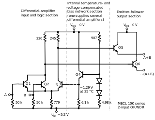
In electronics, emitter-coupled logic (ECL) is a high-speed integrated circuit bipolar transistor logic family. ECL uses an overdriven bipolar junction transistor (BJT) differential amplifier with single-ended input and limited emitter current to avoid the saturated region of operation and its slow turn-off behavior. As the current is steered between two legs of an emitter-coupled pair, ECL is sometimes called current-steering logic (CSL), current-mode logic (CML) or current-switch emitter-follower (CSEF) logic.
The method of logical effort, a term coined by Ivan Sutherland and Bob Sproull in 1991, is a straightforward technique used to estimate delay in a CMOS circuit. Used properly, it can aid in selection of gates for a given function and sizing gates to achieve the minimum delay possible for a circuit.
Resistor–transistor logic (RTL), sometimes also known as transistor–resistor logic (TRL), is a class of digital circuits built using resistors as the input network and bipolar junction transistors (BJTs) as switching devices. RTL is the earliest class of transistorized digital logic circuit; it was succeeded by diode–transistor logic (DTL) and transistor–transistor logic (TTL).
In computer engineering, a logic family is one of two related concepts:

In integrated circuits, depletion-load NMOS is a form of digital logic family that uses only a single power supply voltage, unlike earlier NMOS logic families that needed more than one different power supply voltage. Although manufacturing these integrated circuits required additional processing steps, improved switching speed and the elimination of the extra power supply made this logic family the preferred choice for many microprocessors and other logic elements.
XOR gate is a digital logic gate that gives a true output when the number of true inputs is odd. An XOR gate implements an exclusive or from mathematical logic; that is, a true output results if one, and only one, of the inputs to the gate is true. If both inputs are false (0/LOW) or both are true, a false output results. XOR represents the inequality function, i.e., the output is true if the inputs are not alike otherwise the output is false. A way to remember XOR is "must have one or the other but not both".
Power optimization is the use of electronic design automation tools to optimize (reduce) the power consumption of a digital design, such as that of an integrated circuit, while preserving the functionality.
Diode logic constructs AND and OR logic gates with diodes and resistors.

Integrated injection logic (IIL, I2L, or I2L) is a class of digital circuits built with multiple collector bipolar junction transistors (BJT). When introduced it had speed comparable to TTL yet was almost as low power as CMOS, making it ideal for use in VLSI (and larger) integrated circuits. The gates can be made smaller with this logic family than with CMOS because complementary transistors are not needed. Although the logic voltage levels are very close (High: 0.7V, Low: 0.2V), I2L has high noise immunity because it operates by current instead of voltage. I2L was developed in 1971 by Siegfried K. Wiedmann and Horst H. Berger who originally called it merged-transistor logic (MTL). A disadvantage of this logic family is that the gates draw power when not switching unlike with CMOS.
In integrated circuit design, dynamic logic is a design methodology in combinational logic circuits, particularly those implemented in metal–oxide–semiconductor (MOS) technology. It is distinguished from the so-called static logic by exploiting temporary storage of information in stray and gate capacitances. It was popular in the 1970s and has seen a recent resurgence in the design of high-speed digital electronics, particularly central processing units (CPUs). Dynamic logic circuits are usually faster than static counterparts and require less surface area, but are more difficult to design. Dynamic logic has a higher average rate of voltage transitions than static logic, but the capacitive loads being transitioned are smaller so the overall power consumption of dynamic logic may be higher or lower depending on various tradeoffs. When referring to a particular logic family, the dynamic adjective usually suffices to distinguish the design methodology, e.g. dynamic CMOS or dynamic SOI design.
Multi-threshold CMOS (MTCMOS) is a variation of CMOS chip technology which has transistors with multiple threshold voltages (Vth) in order to optimize delay or power. The Vth of a MOSFET is the gate voltage where an inversion layer forms at the interface between the insulating layer (oxide) and the substrate (body) of the transistor. Low Vth devices switch faster, and are therefore useful on critical delay paths to minimize clock periods. The penalty is that low Vth devices have substantially higher static leakage power. High Vth devices are used on non-critical paths to reduce static leakage power without incurring a delay penalty. Typical high Vth devices reduce static leakage by 10 times compared with low Vth devices.

Domino logic is a CMOS-based evolution of dynamic logic techniques consisting of a dynamic logic gate cascaded into a static CMOS inverter. The term derives from the fact that in domino logic, each stage ripples the next stage for evaluation, similar to dominoes falling one after the other. Domino logic contrasts with other solutions to the cascade problem where cascading is interrupted by clocks or other means.
PMOS or pMOS logic is a family of digital circuits based on p-channel, enhancement mode metal–oxide–semiconductor field-effect transistors (MOSFETs). In the late 1960s and early 1970s, PMOS logic was the dominant semiconductor technology for large-scale integrated circuits before being superseded by NMOS and CMOS devices.
Power gating is a technique used in integrated circuit design to reduce power consumption, by shutting off the current to blocks of the circuit that are not in use. In addition to reducing stand-by or leakage power, power gating has the benefit of enabling Iddq testing.

The memory cell is the fundamental building block of computer memory. The memory cell is an electronic circuit that stores one bit of binary information and it must be set to store a logic 1 and reset to store a logic 0. Its value is maintained/stored until it is changed by the set/reset process. The value in the memory cell can be accessed by reading it.

