Multiplexer

Last updated
Schematic of a 2-to-1 multiplexer. It can be equated to a controlled switch. Multiplexer2.svg
Schematic of a 2-to-1 multiplexer. It can be equated to a controlled switch.
Schematic of a 1-to-2 demultiplexer. Like a multiplexer, it can be equated to a controlled switch. Demultiplexer.png
Schematic of a 1-to-2 demultiplexer. Like a multiplexer, it can be equated to a controlled switch.

In electronics, a multiplexer (or mux; spelled sometimes as multiplexor), also known as a data selector, is a device that selects between several analog or digital input signals and forwards the selected input to a single output line. [1] The selection is directed by a separate set of digital inputs known as select lines. A multiplexer of inputs has select lines, which are used to select which input line to send to the output. [2]

Contents

A multiplexer makes it possible for several input signals to share one device or resource, for example, one analog-to-digital converter or one communications transmission medium, instead of having one device per input signal. Multiplexers can also be used to implement Boolean functions of multiple variables.

Conversely, a demultiplexer (or demux) is a device taking a single input and selecting signals of the output of the compatible mux, which is connected to the single input, and a shared selection line. A multiplexer is often used with a complementary demultiplexer on the receiving end. [1]

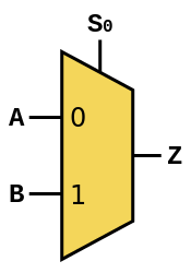
An electronic multiplexer can be considered as a multiple-input, single-output switch, and a demultiplexer as a single-input, multiple-output switch. [3] The schematic symbol for a multiplexer is an isosceles trapezoid with the longer parallel side containing the input pins and the short parallel side containing the output pin. [4] The schematic on the right shows a 2-to-1 multiplexer on the left and an equivalent switch on the right. The wire connects the desired input to the output.

Applications

Multiplexers are part of computer systems to select data from a specific source, be it a memory chip or a hardware peripheral. A computer uses multiplexers to control the data and address buses, allowing the processor to select data from multiple data sources

The basic function of a multiplexer: combining multiple inputs into a single data stream. On the receiving side, a demultiplexer splits the single data stream into the original multiple signals. Telephony multiplexer system.gif
The basic function of a multiplexer: combining multiple inputs into a single data stream. On the receiving side, a demultiplexer splits the single data stream into the original multiple signals.

In digital communications, multiplexers allow several connections over a single channel, by connecting the multiplexer's single output to the demultiplexer's single input (Time-Division Multiplexing). The image to the right demonstrates this benefit. In this case, the cost of implementing separate channels for each data source is higher than the cost and inconvenience of providing the multiplexing/demultiplexing functions.

At the receiving end of the data link a complementary demultiplexer is usually required to break the single data stream back down into the original streams. In some cases, the far end system may have functionality greater than a simple demultiplexer; and while the demultiplexing still occurs technically, it may never be implemented discretely. This would be the case when, for instance, a multiplexer serves a number of IP network users; and then feeds directly into a router, which immediately reads the content of the entire link into its routing processor; and then does the demultiplexing in memory from where it will be converted directly into IP sections.

Often, a multiplexer and demultiplexer are combined into a single piece of equipment, which is simply referred to as a multiplexer. Both circuit elements are needed at both ends of a transmission link because most communications systems transmit in both directions.

In analog circuit design, a multiplexer is a special type of analog switch that connects one signal selected from several inputs to a single output.

Digital multiplexers

In digital circuit design, the selector wires are of digital value. In the case of a 2-to-1 multiplexer, a logic value of 0 would connect to the output while a logic value of 1 would connect to the output. In larger multiplexers, the number of selector pins is equal to where is the number of inputs.

For example, 9 to 16 inputs would require no fewer than 4 selector pins and 17 to 32 inputs would require no fewer than 5 selector pins. The binary value expressed on these selector pins determines the selected input pin.

A 2-to-1 multiplexer has a boolean equation where and are the two inputs, is the selector input, and is the output:

or
A 2-to-1 mux Multiplexer 2-to-1.svg
A 2-to-1 mux

Which can be expressed as a truth table:

0000
0010
0101
0111
1000
1011
1100
1111

Or, in simpler notation:

0A
1B


These tables show that when then but when then . A straightforward realization of this 2-to-1 multiplexer would need 2 AND gates, an OR gate, and a NOT gate. While this is mathematically correct, a direct physical implementation would be prone to race conditions that require additional gates to suppress. [5]

Larger multiplexers are also common and, as stated above, require selector pins for inputs. Other common sizes are 4-to-1, 8-to-1, and 16-to-1. Since digital logic uses binary values, powers of 2 are used (4, 8, 16) to maximally control a number of inputs for the given number of selector inputs.

The boolean equation for a 4-to-1 multiplexer is:

or

Which can be expressed as a truth table:

00A
01B
10C
11D

The following 4-to-1 multiplexer is constructed from 3-state buffers and AND gates (the AND gates are acting as the decoder):

A 4:1 MUX circuit using 3 input AND and other gates 4to1 MUX using basic gates.jpg
A 4:1 MUX circuit using 3 input AND and other gates

Mux from 3 state buffers.png

The subscripts on the inputs indicate the decimal value of the binary control inputs at which that input is let through.

Chaining multiplexers

Larger Multiplexers can be constructed by using smaller multiplexers by chaining them together. For example, an 8-to-1 multiplexer can be made with two 4-to-1 and one 2-to-1 multiplexers. The two 4-to-1 multiplexer outputs are fed into the 2-to-1 with the selector pins on the 4-to-1's put in parallel giving a total number of selector inputs to 3, which is equivalent to an 8-to-1.

List of ICs which provide multiplexing

Signetics S54S157 quad 2:1 mux 54S157 Signetics 8014 package top.jpg
Signetics S54S157 quad 2:1 mux

For 7400 series part numbers in the following table, "x" is the logic family.

IC No.FunctionOutput State
74x157Quad 2:1 mux.Output same as input given
74x158Quad 2:1 mux.Output is inverted input
74x153Dual 4:1 mux.Output same as input
74x352Dual 4:1 mux.Output is inverted input
74x151A8:1 mux.Both outputs available (i.e., complementary outputs)
74x1518:1 mux.Output is inverted input
74x15016:1 mux.Output is inverted input

Digital demultiplexers

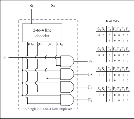
Demultiplexers take one data input and a number of selection inputs, and they have several outputs. They forward the data input to one of the outputs depending on the values of the selection inputs. Demultiplexers are sometimes convenient for designing general-purpose logic because if the demultiplexer's input is always true, the demultiplexer acts as a binary decoder. This means that any function of the selection bits can be constructed by logically OR-ing the correct set of outputs.

If X is the input and S is the selector, and A and B are the outputs:

Example: A Single Bit 1-to-4 Line Demultiplexer Demultiplexer Example01.svg
Example: A Single Bit 1-to-4 Line Demultiplexer

List of ICs which provide demultiplexing

Fairchild 74F138 1:8 demultiplexer ROCKY-518HV - Fairchild 74F138-2387.jpg
Fairchild 74F138 1:8 demultiplexer

For 7400 series part numbers in the following table, "x" is the logic family.

IC No. (7400)IC No. (4000)FunctionOutput State
74x139Dual 1:4 demux.Output is inverted input
74x156Dual 1:4 demux.Output is open collector
74x1381:8 demux.Output is inverted input
74x2381:8 demux.
74x1541:16 demux.Output is inverted input
74x159CD4514/151:16 demux.Output is open collector and same as input

Bi-directional multiplexers

Bi-directional multiplexers are built using analog switches or transmission gates controlled by the select pins. This allows the roles of input and output to be swapped, so that a bi-directional multiplexer can function both as a demultiplexer and multiplexer. [6]

Multiplexers as PLDs

Multiplexers can also be used as programmable logic devices, to implement Boolean functions. Any Boolean function of n variables and one result can be implemented with a multiplexer with n selector inputs. The variables are connected to the selector inputs, and the function result, 0 or 1, for each possible combination of selector inputs is connected to the corresponding data input. If one of the variables (for example, D) is also available inverted, a multiplexer with n-1 selector inputs is sufficient; the data inputs are connected to 0, 1, D, or ~D, according to the desired output for each combination of the selector inputs. [7]

Unconventional use of Multiplexers for arithmetic

Multiplexers also found it foot in unconventional Stochastic Computing (SC) such that it could be used for arithmetic addition. When data is presented as a probability bitstream such that the number of 1's bit represent the magnitude of a value, then the function of a 2-to-1 multiplexer could be presented as a probability function as:

, where a and b are the input bitstream and s is the select input. Using the select input s = 0.5 yields:

It is not an exact addition but a scaled-addition, which is acceptable in most SC studies. It is widely used for average adding, average pooling and median filtering in the SC circuits. More advanced use case for Multiplexer includes Bernstein polynomial function generator [8] , which could generate arbitrary math function in the SC domain. New study also found that Multiplexer combination can perform large-scale multiply-accumulate operation, [9] and it is proven feasable to accelerate convolutional neural network on field-programmable gate array.

See also

Related Research Articles

<span class="mw-page-title-main">Logical conjunction</span> Logical connective AND

In logic, mathematics and linguistics, and is the truth-functional operator of conjunction or logical conjunction. The logical connective of this operator is typically represented as or or (prefix) or or in which is the most modern and widely used.

<span class="mw-page-title-main">Logical connective</span> Symbol connecting sentential formulas in logic

In logic, a logical connective is a logical constant. Connectives can be used to connect logical formulas. For instance in the syntax of propositional logic, the binary connective can be used to join the two atomic formulas and , rendering the complex formula .

<span class="mw-page-title-main">De Morgan's laws</span> Pair of logical equivalences

In propositional logic and Boolean algebra, De Morgan's laws, also known as De Morgan's theorem, are a pair of transformation rules that are both valid rules of inference. They are named after Augustus De Morgan, a 19th-century British mathematician. The rules allow the expression of conjunctions and disjunctions purely in terms of each other via negation.

<span class="mw-page-title-main">Combinational logic</span> Type of digital logic implemented by boolean circuits

In automata theory, combinational logic is a type of digital logic that is implemented by Boolean circuits, where the output is a pure function of the present input only. This is in contrast to sequential logic, in which the output depends not only on the present input but also on the history of the input. In other words, sequential logic has memory while combinational logic does not.

<span class="mw-page-title-main">Inverter (logic gate)</span> Logic gate implementing negation

In digital logic, an inverter or NOT gate is a logic gate which implements logical negation. It outputs a bit opposite of the bit that is put into it. The bits are typically implemented as two differing voltage levels.

<span class="mw-page-title-main">Exclusive or</span> True when either but not both inputs are true

Exclusive or, exclusive disjunction, exclusive alternation, logical non-equivalence, or logical inequality is a logical operator whose negation is the logical biconditional. With two inputs, XOR is true if and only if the inputs differ. With multiple inputs, XOR is true if and only if the number of true inputs is odd.

<span class="mw-page-title-main">Negation</span> Logical operation

In logic, negation, also called the logical not or logical complement, is an operation that takes a proposition to another proposition "not ", standing for " is not true", written , or . It is interpreted intuitively as being true when is false, and false when is true. Negation is thus a unary logical connective. It may be applied as an operation on notions, propositions, truth values, or semantic values more generally. In classical logic, negation is normally identified with the truth function that takes truth to falsity. In intuitionistic logic, according to the Brouwer–Heyting–Kolmogorov interpretation, the negation of a proposition is the proposition whose proofs are the refutations of .

<span class="mw-page-title-main">Logical NOR</span> Binary operation that is true if and only if both operands are false

In Boolean logic, logical NOR, non-disjunction, or joint denial is a truth-functional operator which produces a result that is the negation of logical or. That is, a sentence of the form (p NOR q) is true precisely when neither p nor q is true—i.e. when both p and q are false. It is logically equivalent to and , where the symbol signifies logical negation, signifies OR, and signifies AND.

In logic, a truth function is a function that accepts truth values as input and produces a unique truth value as output. In other words: the input and output of a truth function are all truth values; a truth function will always output exactly one truth value, and inputting the same truth value(s) will always output the same truth value. The typical example is in propositional logic, wherein a compound statement is constructed using individual statements connected by logical connectives; if the truth value of the compound statement is entirely determined by the truth value(s) of the constituent statement(s), the compound statement is called a truth function, and any logical connectives used are said to be truth functional.

In digital electronics, a NAND gate (NOT-AND) is a logic gate which produces an output which is false only if all its inputs are true; thus its output is complement to that of an AND gate. A LOW (0) output results only if all the inputs to the gate are HIGH (1); if any input is LOW (0), a HIGH (1) output results. A NAND gate is made using transistors and junction diodes. By De Morgan's laws, a two-input NAND gate's logic may be expressed as , making a NAND gate equivalent to inverters followed by an OR gate.

XOR gate is a digital logic gate that gives a true output when the number of true inputs is odd. An XOR gate implements an exclusive or from mathematical logic; that is, a true output results if one, and only one, of the inputs to the gate is true. If both inputs are false (0/LOW) or both are true, a false output results. XOR represents the inequality function, i.e., the output is true if the inputs are not alike otherwise the output is false. A way to remember XOR is "must have one or the other but not both".

The NAND Boolean function has the property of functional completeness. This means that any Boolean expression can be re-expressed by an equivalent expression utilizing only NAND operations. For example, the function NOT(x) may be equivalently expressed as NAND(x,x). In the field of digital electronic circuits, this implies that it is possible to implement any Boolean function using just NAND gates.

The XNOR gate is a digital logic gate whose function is the logical complement of the Exclusive OR (XOR) gate. It is equivalent to the logical connective from mathematical logic, also known as the material biconditional. The two-input version implements logical equality, behaving according to the truth table to the right, and hence the gate is sometimes called an "equivalence gate". A high output (1) results if both of the inputs to the gate are the same. If one but not both inputs are high (1), a low output (0) results.

In logic, a functionally complete set of logical connectives or Boolean operators is one that can be used to express all possible truth tables by combining members of the set into a Boolean expression. A well-known complete set of connectives is { AND, NOT }. Each of the singleton sets { NAND } and { NOR } is functionally complete. However, the set { AND, OR } is incomplete, due to its inability to express NOT.

<span class="mw-page-title-main">Boolean circuit</span> Model of computation

In computational complexity theory and circuit complexity, a Boolean circuit is a mathematical model for combinational digital logic circuits. A formal language can be decided by a family of Boolean circuits, one circuit for each possible input length.

Logic optimization is a process of finding an equivalent representation of the specified logic circuit under one or more specified constraints. This process is a part of a logic synthesis applied in digital electronics and integrated circuit design.

<span class="mw-page-title-main">Karnaugh map</span> Graphical method to simplify Boolean expressions

The Karnaugh map is a method of simplifying Boolean algebra expressions. Maurice Karnaugh introduced it in 1953 as a refinement of Edward W. Veitch's 1952 Veitch chart, which was a rediscovery of Allan Marquand's 1881 logical diagram aka Marquand diagram but with a focus now set on its utility for switching circuits. Veitch charts are also known as Marquand–Veitch diagrams or, rarely, as Svoboda charts, and Karnaugh maps as Karnaugh–Veitch maps.

<span class="mw-page-title-main">Intel 8255</span> Programmable Peripheral Interface chip

The Intel 8255 Programmable Peripheral Interface (PPI) chip was developed and manufactured by Intel in the first half of the 1970s for the Intel 8080 microprocessor. The 8255 provides 24 parallel input/output lines with a variety of programmable operating modes.

The Tseytin transformation, alternatively written Tseitin transformation, takes as input an arbitrary combinatorial logic circuit and produces an equisatisfiable boolean formula in conjunctive normal form (CNF). The length of the formula is linear in the size of the circuit. Input vectors that make the circuit output "true" are in 1-to-1 correspondence with assignments that satisfy the formula. This reduces the problem of circuit satisfiability on any circuit to the satisfiability problem on 3-CNF formulas. It was discovered by the Russian scientist Grigori Tseitin.

In mathematics and mathematical logic, Boolean algebra is a branch of algebra. It differs from elementary algebra in two ways. First, the values of the variables are the truth values true and false, usually denoted 1 and 0, whereas in elementary algebra the values of the variables are numbers. Second, Boolean algebra uses logical operators such as conjunction (and) denoted as , disjunction (or) denoted as , and the negation (not) denoted as ¬. Elementary algebra, on the other hand, uses arithmetic operators such as addition, multiplication, subtraction, and division. Boolean algebra is therefore a formal way of describing logical operations, in the same way that elementary algebra describes numerical operations.

References

  1. 1 2 Dean, Tamara (2010). Network+ Guide to Networks. Delmar. pp. 82–85. ISBN   978-1423902454.
  2. Debashis, De (2010). Basic Electronics. Dorling Kindersley. p. 557. ISBN   9788131710685.
  3. Lipták, Béla (2002). Instrument engineers' handbook: Process software and digital networks. CRC Press. p. 343. ISBN   9781439863442.
  4. Harris, David (2007). Digital Design and Computer Architecture. Penrose. p. 79. ISBN   9780080547060.
  5. Crowe, John; Hayes-Gill, Barrie (1998). "The multiplexer hazard". Introduction to Digital Electronics. Elsevier. pp. 111–3. ISBN   9780080534992.
  6. "Are switches & multiplexers bidirectional? | Video | TI.com". Texas Instruments . Retrieved 2023-08-03.
  7. Lancaster, Donald E. (1974). The TTL Cookbook. H.W. Sams. pp. 140–3. ISBN   9780672210358.
  8. Najafi, M. Hassan; Li, Peng; Lilja, David J.; Qian, Weikang; Bazargan, Kia; Riedel, Marc (2017-06-29). "A Reconfigurable Architecture with Sequential Logic-Based Stochastic Computing". ACM Journal on Emerging Technologies in Computing Systems. 13 (4): 57:1–57:28. doi:10.1145/3060537. ISSN   1550-4832.
  9. Lee, Yang Yang; Halim, Zaini Abdul; Wahab, Mohd Nadhir Ab; Almohamad, Tarik Adnan (2024-03-04). "Stochastic Computing Convolutional Neural Network Architecture Reinvented for Highly Efficient Artificial Intelligence Workload on Field-Programmable Gate Array". Research. 7. doi:10.34133/research.0307. ISSN   2639-5274. PMC   10911856 . PMID   38439995.

Further reading