SuperH

Last updated
SuperH (SH)
Designer Hitachi
Bits32-bit (32 → 64)
Introduced1992 [1]
Design RISC
Encoding SH-2: 16-bit instructions
SH-2A and newer: mixed 16- and 32-bit instructions
Endianness Bi
OpenYes, and royalty-free [2]

SuperH (or SH) is a 32-bit reduced instruction set computing (RISC) instruction set architecture (ISA) developed by Hitachi and currently produced by Renesas. It is implemented by microcontrollers and microprocessors for embedded systems.

Contents

At the time of introduction, SuperH was notable for having fixed-length 16-bit instructions in spite of its 32-bit architecture. Using smaller instructions had consequences: the register file was smaller and instructions were generally two-operand format. However for the market the SuperH was aimed at, this was a small price to pay for the improved memory and processor cache efficiency.

Later versions of the design, starting with SH-5, included both 16- and 32-bit instructions, with the 16-bit versions mapping onto the 32-bit version inside the CPU. This allowed the machine code to continue using the shorter instructions to save memory, while not demanding the amount of instruction decoding logic needed if they were completely separate instructions. This concept is now known as a compressed instruction set and is also used by other companies, the most notable example being ARM for its Thumb instruction set.

In 2015, many of the original patents for the SuperH architecture expired and the SH-2 CPU was reimplemented as open source hardware under the name J2.

History

SH-1 and SH-2

SH-2 on Sega 32X and Sega Saturn HD6417095 01.jpg
SH-2 on Sega 32X and Sega Saturn

The SuperH processor core family was first developed by Hitachi in the early 1990s. The design concept was for a single instruction set (ISA) that would be upward compatible across a series of CPU cores.

In the past, this sort of design problem would have been solved using microcode, with the low-end models in the series performing non-implemented instructions as a series of more basic instructions. For instance, a "long multiply" (multiplying two 32-bit registers to produce a 64-bit product) might be implemented in hardware on high-end models but instead be performed as a series of additions on low-end models.

One of the key realizations during the development of the RISC concept was that the microcode had a finite decoding time, and as processors became faster, this represented an unacceptable performance overhead. To address this, Hitachi instead developed a single ISA for the entire line, with unsupported instructions causing traps on those implementations that didn't include hardware support. For instance, the initial models in the line, the SH-1 and SH-2, differed only in their support for 64-bit multiplication; the SH-2 supported MUL, DMULS and DMULU, whereas the SH-1 would cause a trap if these were encountered. [3]

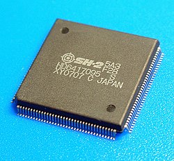
The SH-1 was the basic model, supporting a total of 56 instructions. The SH-2 added 64-bit multiplication and a few additional commands for branching and other duties, bringing the total to 62 supported instructions. [3] The SH-1 and the SH-2 were used in the Sega Saturn, Sega 32X and Capcom CPS-3. [4]

The ISA uses 16-bit instructions for better code density than 32-bit instructions, which was important at the time due to the high cost of main memory and the implementation cost of cache. As of 2023, code density is still important for small embedded systems and massively multicore processors. The downsides to this approach were that there were fewer bits available to encode a register number or a constant value. In the original SuperH ISA, there were only 16 general registers, requiring four bits for the source and another four for the destination; however some instructions have an implied R0, R15, or a system register as an extra operand. The instruction opcode is four, eight, twelve, or sixteen bits long, and the remaining four-bit fields are used for register or immediate operands in various ways: there are twelve classes of instructions, for a total of 142 instructions in SH-2. [5]

Delayed branches are introduced for both SH-1 and SH-2. Unconditional branch instructions have one delay slot. [6]

SH-3

A few years later, the SH-3 core was added to the family; new features included another interrupt concept, a memory management unit (MMU), and a modified cache concept. These features required an extended instruction set, adding six new instructions for a total of 68. [3] The SH-3 was bi-endian, running in either big-endian or little-endian byte ordering.

The SH-3 core also added a DSP extension, then called SH-3-DSP. With extended data paths for efficient DSP processing, special accumulators and a dedicated MAC-type DSP engine, this core unified the DSP and the RISC processor world. A derivative of the DSP was also used with the original SH-2 core.

Between 1994 and 1996, 35.1 million SuperH devices were shipped worldwide. [7]

SH-4

In 1997, Hitachi and STMicroelectronics (STM) started collaborating on the design of the SH-4 for the Dreamcast. SH-4 featured superscalar (2-way) instruction execution and a vector floating-point unit (particularly suited to 3D graphics). Standard chips based on the SH-4 were introduced around 1998. [8]

Licensing

In early 2001, Hitachi and STM formed the IP company SuperH, Inc., which was going to license the SH-4 core to other companies and was developing the SH-5 architecture, the first move of SuperH into the 64-bit area. The earlier SH-1 through 3 remained the property of Hitachi. [8] [9]

In 2003, Hitachi and Mitsubishi Electric formed a joint-venture called Renesas Technology, with Hitachi controlling 55% of it. In 2004, Renesas Technology bought STMicroelectronics's share of ownership in the SuperH Inc. and with it the licence to the SH cores. [10] Renesas Technology later became Renesas Electronics, following their merger with NEC Electronics.

The SH-5 design supported two modes of operation: SHcompact mode, which is equivalent to the user-mode instructions of the SH-4 instruction set; and SHmedia mode, which is very different in that it uses 32-bit instructions with sixty-four 64-bit integer registers and SIMD instructions. In SHmedia mode the destination of a branch (jump) is loaded into a branch register separately from the actual branch instruction. This allows the processor to prefetch instructions for a branch without having to snoop the instruction stream. The combination of a compact 16-bit instruction encoding with a more powerful 32-bit instruction encoding is not unique to SH-5; ARM processors have a 16-bit Thumb mode (ARM licensed several patents from SuperH for Thumb [11] ) and MIPS processors have a MIPS-16 mode. However, SH-5 differs because its backward compatibility mode is the 16-bit encoding rather than the 32-bit encoding.

The last evolutionary step happened around 2003 where the cores from SH-2 up to SH-4 were getting unified into a superscalar SH-X core which formed a kind of instruction set superset of the previous architectures, and added support for symmetric multiprocessing.

Continued availability

Since 2010, the SuperH CPU cores, architecture and products are with Renesas Electronics and the architecture is consolidated around the SH-2, SH-2A, SH-3, SH-4 and SH-4A platforms. The system-on-chip products based on SH-3, SH-4 and SH-4A microprocessors were subsequently replaced by newer generations based on licensed CPU cores from Arm Ltd., with many of the existing models still marketed and sold until March 2025 through the Renesas Product Longevity Program. [12]

As of 2021, the SH72xx microcontrollers based on the SH-2A continue to be marketed by Renesas with guaranteed availability until February 2029, along with newer products based on several other architectures including Arm, RX, and RH850.

J Core

The last of the SH-2 patents expired in 2014. At LinuxCon Japan 2015, j-core developers presented a cleanroom reimplemention of the SH-2 ISA with extensions (known as the "J2 core" due to the unexpired trademarks). [11] [13] Subsequently, a design walkthrough was presented at ELC 2016. [14]

The open source BSD-licensed VHDL code for the J2 core has been proven on Xilinx FPGAs and on ASICs manufactured on TSMC's 180 nm process, and is capable of booting µClinux. [11] J2 is backwards ISA compatible with SH-2, implemented as a 5-stage pipeline with separate Instruction and Data memory interfaces, and a machine-generated Instruction Decoder supporting the densely packed and complex (relative to other RISC machines) ISA. Additional instructions are easy to add. J2 implements instructions for dynamic shift (using the SH-3 and later instruction patterns), extended atomic operations (used for threading primitives) and locking/interfaces for symmetric multiprocessor support. Plans to implement the SH-2A (as "J2+") and SH-4 (as "J4") instruction sets as the relevant patents expire in 2016–2017. [11] [ needs update ]

Several features of SuperH have been cited as motivations for designing new cores based on this architecture: [11]

Models

Hitachi SH-3 CPU Hitachi SH3.jpg
Hitachi SH-3 CPU

The family of SuperH CPU cores includes:

SH-2

Hitachi SH-2 CPU Denso-SH2.jpg
Hitachi SH-2 CPU

The SH-2 is a 32-bit RISC architecture with a 16-bit fixed instruction length for high code density and features a hardware multiply–accumulate (MAC) block for DSP algorithms and has a five-stage pipeline.

The SH-2 has a cache on all ROM-less devices.

It provides 16 general-purpose registers, a vector-base register, global-base register, and a procedure register.

Today the SH-2 family stretches from 32 KB of on-board flash up to ROM-less devices. It is used in a variety of different devices with differing peripherals such as CAN, Ethernet, motor-control timer unit, fast ADC and others.

SH-2A

The SH-2A is an upgrade to the SH-2 core that added some 32-bit instructions. It was announced in early 2006.

New features on the SH-2A core include:

The SH-2A family today spans a wide memory field from 16 KB up to and includes many ROM-less variations. The devices feature standard peripherals such as CAN, Ethernet, USB and more as well as more application-specific peripherals such as motor control timers, TFT controllers and peripherals dedicated to automotive powertrain applications.

SH-4

Hitachi SH-4 CPU SH7091 01.jpg
Hitachi SH-4 CPU

The SH-4 is a RISC CPU and was developed for primary use in multimedia applications, such as Sega's Dreamcast and NAOMI game systems. It includes a much more powerful floating-point unit [note] and additional built-in functions, along with the standard 32-bit integer processing and 16-bit instruction size.

SH-4 features include:

^ There is no FPU in the custom SH-4 made for Casio, the SH7305.

SH-5

The SH-5 is a 64-bit RISC CPU. [17]

Almost no non-simulated SH-5 hardware was ever released, [18] and, unlike the still-live SH-4, support for SH-5 was dropped from GCC [19] and Linux.

Related Research Articles

<span class="mw-page-title-main">PA-RISC</span> Instruction set architecture by Hewlett-Packard

Precision Architecture RISC (PA-RISC) or Hewlett Packard Precision Architecture, is a general purpose computer instruction set architecture (ISA) developed by Hewlett-Packard from the 1980s until the 2000s.

<span class="mw-page-title-main">Reduced instruction set computer</span> Processor executing one instruction in minimal clock cycles

In electronics and computer science, a reduced instruction set computer (RISC) is a computer architecture designed to simplify the individual instructions given to the computer to accomplish tasks. Compared to the instructions given to a complex instruction set computer (CISC), a RISC computer might require more instructions in order to accomplish a task because the individual instructions are written in simpler code. The goal is to offset the need to process more instructions by increasing the speed of each instruction, in particular by implementing an instruction pipeline, which may be simpler to achieve given simpler instructions.

In computer science, an instruction set architecture (ISA) is a part of the abstract model of a computer, which generally defines how software controls the CPU. A device that executes instructions described by that ISA, such as a central processing unit (CPU), is called an implementation.

Very long instruction word (VLIW) refers to instruction set architectures that are designed to exploit instruction level parallelism (ILP). A VLIW processor allows programs to explicitly specify instructions to execute in parallel, whereas conventional central processing units (CPUs) mostly allow programs to specify instructions to execute in sequence only. VLIW is intended to allow higher performance without the complexity inherent in some other designs.

ARM is a family of RISC instruction set architectures (ISAs) for computer processors. Arm Ltd. develops the ISAs and licenses them to other companies, who build the physical devices that use the instruction set. It also designs and licenses cores that implement these ISAs.

The Motorola 68000 series is a family of 32-bit complex instruction set computer (CISC) microprocessors. During the 1980s and early 1990s, they were popular in personal computers and workstations and were the primary competitors of Intel's x86 microprocessors. They were best known as the processors used in the early Apple Macintosh, the Sharp X68000, the Commodore Amiga, the Sinclair QL, the Atari ST and Falcon, the Atari Jaguar, the Sega Genesis and Sega CD, the Philips CD-i, the Capcom System I (Arcade), the AT&T UNIX PC, the Tandy Model 16/16B/6000, the Sun Microsystems Sun-1, Sun-2 and Sun-3, the NeXT Computer, NeXTcube, NeXTstation, and NeXTcube Turbo, early Silicon Graphics IRIS workstations, the Aesthedes, computers from MASSCOMP, the Texas Instruments TI-89/TI-92 calculators, the Palm Pilot, the Control Data Corporation CDCNET Device Interface, and the Space Shuttle. Although no modern desktop computers are based on processors in the 680x0 series, derivative processors are still widely used in embedded systems.

<span class="mw-page-title-main">Intel i960</span> RISC-based microprocessor design

Intel's i960 was a RISC-based microprocessor design that became popular during the early 1990s as an embedded microcontroller. It became a best-selling CPU in that segment, along with the competing AMD 29000. In spite of its success, Intel stopped marketing the i960 in the late 1990s, as a result of a settlement with DEC whereby Intel received the rights to produce the StrongARM CPU. The processor continues to be used for a few military applications.

<span class="mw-page-title-main">Blackfin</span> Family of 16-/32-bit microprocessors

The Blackfin is a family of 16-/32-bit microprocessors developed, manufactured and marketed by Analog Devices. The processors have built-in, fixed-point digital signal processor (DSP) functionality performed by 16-bit multiply–accumulates (MACs), accompanied on-chip by a microcontroller. It was designed for a unified low-power processor architecture that can run operating systems while simultaneously handling complex numeric tasks such as real-time H.264 video encoding.

The POWER1 is a multi-chip CPU developed and fabricated by IBM that implemented the POWER instruction set architecture (ISA). It was originally known as the RISC System/6000 CPU or, when in an abbreviated form, the RS/6000 CPU, before introduction of successors required the original name to be replaced with one that used the same naming scheme (POWERn) as its successors in order to differentiate it from the newer designs.

V850 is a 32-bit RISC CPU architecture produced by Renesas Electronics for embedded microcontrollers. It was designed by NEC as a replacement for their earlier NEC V60 family, and was introduced shortly before NEC sold their designs to Renesas in the early 1990s. It has continued to be developed by Renesas as of 2018.

<span class="mw-page-title-main">AVR32</span>

AVR32 is a 32-bit RISC microcontroller architecture produced by Atmel. The microcontroller architecture was designed by a handful of people educated at the Norwegian University of Science and Technology, including lead designer Øyvind Strøm and CPU architect Erik Renno in Atmel's Norwegian design center.

<span class="mw-page-title-main">NEC V60</span> CISC microprocessor

The NEC V60 is a CISC microprocessor manufactured by NEC starting in 1986. Several improved versions were introduced with the same instruction set architecture (ISA), the V70 in 1987, and the V80 and AFPP in 1989. They were succeeded by the V800 product families, which is currently produced by Renesas Electronics.

<span class="mw-page-title-main">History of general-purpose CPUs</span>

The history of general-purpose CPUs is a continuation of the earlier history of computing hardware.

<span class="mw-page-title-main">OpenRISC 1200</span> Open source microprocessor

The OpenRISC 1200 (OR1200) is an implementation of the open source OpenRISC 1000 RISC architecture.

RISC-V is an open standard instruction set architecture (ISA) based on established reduced instruction set computer (RISC) principles. Unlike most other ISA designs, RISC-V is provided under royalty-free open-source licenses. Many companies are offering or have announced RISC-V hardware; open source operating systems with RISC-V support are available, and the instruction set is supported in several popular software toolchains.

Since 1985, many processors implementing some version of the MIPS architecture have been designed and used widely.

<span class="mw-page-title-main">Power ISA</span> Computer instruction set architecture

Power ISA is a reduced instruction set computer (RISC) instruction set architecture (ISA) currently developed by the OpenPOWER Foundation, led by IBM. It was originally developed by IBM and the now-defunct Power.org industry group. Power ISA is an evolution of the PowerPC ISA, created by the mergers of the core PowerPC ISA and the optional Book E for embedded applications. The merger of these two components in 2006 was led by Power.org founders IBM and Freescale Semiconductor.

A compressed instruction set, or simply compressed instructions, are a variation on a microprocessor's instruction set architecture (ISA) that allows instructions to be represented in a more compact format. In most real-world examples, compressed instructions are 16 bits long in a processor that would otherwise use 32-bit instructions. The 16-bit ISA is a subset of the full 32-bit ISA, not a separate instruction set. The smaller format requires some tradeoffs: generally, there are fewer instructions available, and fewer processor registers can be used.

References

Citations

  1. "The Story of the Hitachi SH-2 and the Sega Saturn". www.sega-16.com. Renesas. Retrieved 27 February 2023.
  2. J-core Open Processor
  3. 1 2 3 Program 1996, p. 1.
  4. "CP System III (CPS3) Hardware (Capcom)". www.system16.com. System 16. Retrieved 3 August 2019.
  5. Program 1996, pp. 30–33.
  6. "SH7020 and SH7021 Hardware ManualSuperH™ RISC engine". p. 19,48. Retrieved 2023-12-02.
  7. "360-MIPS SuperH RISC Processor Enables Personal Access Systems SH7750 Launches the SH-4 Series". November 1997. Archived from the original on 5 March 2016.
  8. 1 2 "STMicro, Hitachi plan new company to develop RISC cores". EE Times. 3 April 2001. Hitachi created the SH family of processors and developed its first four major iterations, but has worked with ST since 1997, when the companies agreed to share a common high-end microprocessor road map. They jointly developed the 32-bit SH4 RISC processor core, and began development of the SH5 architecture, which will now be completed by SuperH. SuperH's initial product will be the SH4 core. Earlier SH versions will not be part of the spin-off agreement.
  9. "SuperH, Inc. formed by Hitachi and STMicroelectronics to Boost the Proliferation of SuperH Cores in Embedded Microprocessor Applications".[ dead link ]
  10. Clarke, Peter (28 September 2004). "Renesas to take over SuperH core business". EE Times.
  11. 1 2 3 4 5 Nathan Willis (June 10, 2015). "Resurrecting the SuperH architecture". LWN.net.
  12. ""SuperH RISC Engine Family MCUs"". Renesas Electronics.
  13. 1 2 "J Cores". j-core. Archived from the original on May 11, 2016. Retrieved April 27, 2016.
  14. "j-core Design Walkthrough" (PDF). Archived (PDF) from the original on 2016-06-17.
  15. V.M. Weaver (17 March 2015). "Exploring the Limits of Code Density (Tech Report with Newest Results)" (PDF). Archived (PDF) from the original on 2015-07-13.
  16. Kuwabara, M. (25 July 2019). "Korg EMX / ESX Service Manual" (PDF). Archived from the original (PDF) on 13 July 2019.
  17. "SH-5 CPU Core, Volume1: Architecture" (PDF). Archived (PDF) from the original on 2009-03-20.
  18. "Wasabi SH-5 Press Release". 8 March 2016.
  19. "GCC 7 Release Series Changes, New Features, and Fixes". 2 February 2018.

Bibliography