Related Research Articles
Processor design is a subfield of computer science and computer engineering (fabrication) that deals with creating a processor, a key component of computer hardware.

The 68HC11 is an 8-bit microcontroller (µC) family introduced by Motorola Semiconductor in 1984. It descended from the Motorola 6800 microprocessor by way of the 6801. The 68HC11 devices are more powerful and more expensive than the 68HC08 microcontrollers, and are used in automotive applications, barcode readers, hotel card key writers, amateur robotics, and various other embedded systems. The MC68HC11A8 was the first microcontroller to include CMOS EEPROM.
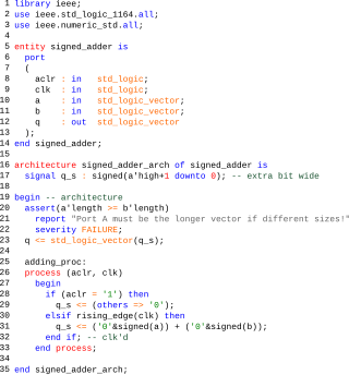
The VHSIC Hardware Description Language (VHDL) is a hardware description language (HDL) that can model the behavior and structure of digital systems at multiple levels of abstraction, ranging from the system level down to that of logic gates, for design entry, documentation, and verification purposes. Since 1987, VHDL has been standardized by the Institute of Electrical and Electronics Engineers (IEEE) as IEEE Std 1076; the latest version of which is IEEE Std 1076-2019. To model analog and mixed-signal systems, an IEEE-standardized HDL based on VHDL called VHDL-AMS has been developed.
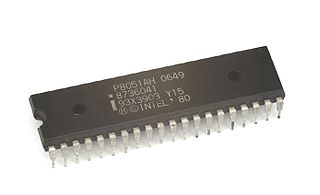
The Intel MCS-51 is a single chip microcontroller (MCU) series developed by Intel in 1980 for use in embedded systems. The architect of the Intel MCS-51 instruction set was John H. Wharton. Intel's original versions were popular in the 1980s and early 1990s, and enhanced binary compatible derivatives remain popular today. It is a complex instruction set computer, but also has some of the features of RISC architectures, such as a large register set and register windows, and has separate memory spaces for program instructions and data.
AVR is a family of microcontrollers developed since 1996 by Atmel, acquired by Microchip Technology in 2016. These are modified Harvard architecture 8-bit RISC single-chip microcontrollers. AVR was one of the first microcontroller families to use on-chip flash memory for program storage, as opposed to one-time programmable ROM, EPROM, or EEPROM used by other microcontrollers at the time.
SuperH is a 32-bit reduced instruction set computing (RISC) instruction set architecture (ISA) developed by Hitachi and currently produced by Renesas. It is implemented by microcontrollers and microprocessors for embedded systems.
JTAG is an industry standard for verifying designs and testing printed circuit boards after manufacture.
LEON is a radiation-tolerant 32-bit central processing unit (CPU) microprocessor core that implements the SPARC V8 instruction set architecture (ISA) developed by Sun Microsystems. It was originally designed by the European Space Research and Technology Centre (ESTEC), part of the European Space Agency (ESA), without any involvement by Sun. Later versions have been designed by Gaisler Research, under a variety of owners. It is described in synthesizable VHSIC Hardware Description Language (VHDL). LEON has a dual license model: An GNU Lesser General Public License (LGPL) and GNU General Public License (GPL) free and open-source software (FOSS) license that can be used without licensing fee, or a proprietary license that can be purchased for integration in a proprietary product. The core is configurable through VHDL generics, and is used in system on a chip (SOC) designs both in research and commercial settings.
Nios II is a 32-bit embedded processor architecture designed specifically for the Altera family of field-programmable gate array (FPGA) integrated circuits. Nios II incorporates many enhancements over the original Nios architecture, making it more suitable for a wider range of embedded computing applications, from digital signal processing (DSP) to system-control.
The MicroBlaze is a soft microprocessor core designed for Xilinx field-programmable gate arrays (FPGA). As a soft-core processor, MicroBlaze is implemented entirely in the general-purpose memory and logic fabric of Xilinx FPGAs.

The Western Design Center (WDC) 65C02 microprocessor is an enhanced CMOS version of the popular nMOS-based 8-bit MOS Technology 6502. It uses less power than the original 6502, fixes several problems, and adds new instructions. The power usage is on the order of 10 to 20 times less than the original 6502 running at the same speed; its reduced power consumption has made it useful in portable computer roles and industrial microcontroller systems. The 65C02 has also been used in some home computers, as well as in embedded applications, including medical-grade implanted devices.

The Parallax P8X32A Propeller is a multi-core processor parallel computer architecture microcontroller chip with eight 32-bit reduced instruction set computer (RISC) central processing unit (CPU) cores. Introduced in 2006, it is designed and sold by Parallax, Inc.

Minimig is an open source re-implementation of an Amiga 500 using a field-programmable gate array (FPGA).
The XAP processor is a RISC processor architecture developed by Cambridge Consultants since 1994. XAP processors are a family of 16-bit and 32-bit cores, all of which are intended for use in an application-specific integrated circuit or ASIC chip design. XAP processors were designed for use in mixed-signal integrated circuits for sensor or wireless applications including Bluetooth, Zigbee, GPS, RFID or Near Field Communication chips. Typically, these integrated circuits are used in low-cost, high-volume products that are battery-powered and must have low energy consumption. There are other applications where XAP processors have been used to good effect, such as wireless sensor networks and medical devices, e.g. hearing aids.
LatticeMico32 is a 32-bit microprocessor reduced instruction set computer (RISC) soft core from Lattice Semiconductor optimized for field-programmable gate arrays (FPGAs). It uses a Harvard architecture, which means the instruction and data buses are separate. Bus arbitration logic can be used to combine the two buses, if desired.

The ARM Cortex-M is a group of 32-bit RISC ARM processor cores licensed by ARM Limited. These cores are optimized for low-cost and energy-efficient integrated circuits, which have been embedded in tens of billions of consumer devices. Though they are most often the main component of microcontroller chips, sometimes they are embedded inside other types of chips too. The Cortex-M family consists of Cortex-M0, Cortex-M0+, Cortex-M1, Cortex-M3, Cortex-M4, Cortex-M7, Cortex-M23, Cortex-M33, Cortex-M35P, Cortex-M55, Cortex-M85. A floating-point unit (FPU) option is available for Cortex-M4 / M7 / M33 / M35P / M55 / M85 cores, and when included in the silicon these cores are sometimes known as "Cortex-MxF", where 'x' is the core variant.
RISC-V is an open standard instruction set architecture (ISA) based on established reduced instruction set computer (RISC) principles. Unlike most other ISA designs, RISC-V is provided under royalty-free open-source licenses. Many companies are offering or have announced RISC-V hardware; open source operating systems with RISC-V support are available, and the instruction set is supported in several popular software toolchains.
The ZPU is a microprocessor stack machine designed by Norwegian company Zylin AS to run supervisory code in electronic systems that include a field-programmable gate array (FPGA).
The Simple-As-Possible (SAP) computer is a simplified computer architecture designed for educational purposes and described in the book Digital Computer Electronics by Albert Paul Malvino and Jerald A. Brown. The SAP architecture serves as an example in Digital Computer Electronics for building and analyzing complex logical systems with digital electronics.
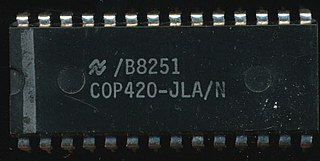
The COP400 or COP II is a 4-bit microcontroller family introduced in 1977 by National Semiconductor as a follow-on product to their original PMOS COP microcontroller. COP400 family members are complete microcomputers containing internal timing, logic, ROM, RAM, and I/O necessary to implement dedicated controllers. Some COP400 devices were second-sourced by Western Digital as the WD4200 family. In the Soviet Union several COP400 microcontrollers were manufactured as the 1820 series.
References
- Notes
- ↑ "PicoBlaze 8-bit Microcontroller" (PDF). Xilinx, Inc. Retrieved 2007-06-25.
- ↑ "PicoBlaze 8-bit Embedded Microcontroller User Guide" (PDF). Xilinx, Inc. Archived from the original (PDF) on 2007-09-27. Retrieved 2007-06-25.
- ↑ Pong P. Chu (2008). FPGA Prototyping by VHDL Examples: Xilinx Spartan-3 Version. Wiley & Sons. ISBN 978-0-470-18531-5.
- Bibliography
- Ivanov Vl. Using a PicoBlaze Processor to Traffic Light Control. Cybernetics and Information Technologies, 15, 5, Marin Drinov, 2015, Online ISSN 1314-4081, doi : 10.1515/cait-2015-0023, pp. 131 – 139. SJR:0.212