Related Research Articles
Processor design is a subfield of computer science and computer engineering (fabrication) that deals with creating a processor, a key component of computer hardware.
A field-programmable gate array (FPGA) is an integrated circuit designed to be configured after manufacturing. The FPGA configuration is generally specified using a hardware description language (HDL), similar to that used for an application-specific integrated circuit (ASIC). Circuit diagrams were previously used to specify the configuration, but this is increasingly rare due to the advent of electronic design automation tools.

A programmable logic device (PLD) is an electronic component used to build reconfigurable digital circuits. Unlike digital logic constructed using discrete logic gates with fixed functions, a PLD has an undefined function at the time of manufacture. Before the PLD can be used in a circuit it must be programmed to implement the desired function. Compared to fixed logic devices, programmable logic devices simplify the design of complex logic and may offer superior performance. Unlike for microprocessors, programming a PLD changes the connections made between the gates in the device.

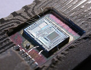
An application-specific integrated circuit is an integrated circuit (IC) chip customized for a particular use, rather than intended for general-purpose use, such as a chip designed to run in a digital voice recorder or a high-efficiency video codec. Application-specific standard product chips are intermediate between ASICs and industry standard integrated circuits like the 7400 series or the 4000 series. ASIC chips are typically fabricated using metal–oxide–semiconductor (MOS) technology, as MOS integrated circuit chips.
Reconfigurable computing is a computer architecture combining some of the flexibility of software with the high performance of hardware by processing with very flexible high speed computing fabrics like field-programmable gate arrays (FPGAs). The principal difference when compared to using ordinary microprocessors is the ability to make substantial changes to the datapath itself in addition to the control flow. On the other hand, the main difference from custom hardware, i.e. application-specific integrated circuits (ASICs) is the possibility to adapt the hardware during runtime by "loading" a new circuit on the reconfigurable fabric.

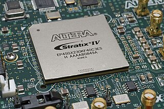
Altera Corporation was a manufacturer of programmable logic devices (PLDs) headquartered in San Jose, California. It was founded in 1983 and acquired by Intel in 2015.
A gate array is an approach to the design and manufacture of application-specific integrated circuits (ASICs) using a prefabricated chip with components that are later interconnected into logic devices according to custom order by adding metal interconnect layers in the factory. It was popular during the upheaval in the semiconductor industry in the 1980s, and its usage declined by the end of the 1990s.

A complex programmable logic device (CPLD) is a programmable logic device with complexity between that of PALs and FPGAs, and architectural features of both. The main building block of the CPLD is a macrocell, which contains logic implementing disjunctive normal form expressions and more specialized logic operations.
In electronic design, a semiconductor intellectual property core, IP core, or IP block is a reusable unit of logic, cell, or integrated circuit layout design that is the intellectual property of one party. IP cores can be licensed to another party or owned and used by a single party. The term comes from the licensing of the patent or source code copyright that exists in the design. Designers of system on chip (SoC), application-specific integrated circuits (ASIC) and systems of field-programmable gate array (FPGA) logic can use IP cores as building blocks.

Hardware acceleration is the use of computer hardware designed to perform specific functions more efficiently when compared to software running on a general-purpose central processing unit (CPU). Any transformation of data that can be calculated in software running on a generic CPU can also be calculated in custom-made hardware, or in some mix of both.
In integrated circuit design, hardware emulation is the process of imitating the behavior of one or more pieces of hardware with another piece of hardware, typically a special purpose emulation system. The emulation model is usually based on a hardware description language source code, which is compiled into the format used by emulation system. The goal is normally debugging and functional verification of the system being designed. Often an emulator is fast enough to be plugged into a working target system in place of a yet-to-be-built chip, so the whole system can be debugged with live data. This is a specific case of in-circuit emulation.
A field-programmable analog array (FPAA) is an integrated circuit device containing computational analog blocks (CAB) and interconnects between these blocks offering field-programmability. Unlike their digital cousin, the FPGA, the devices tend to be more application driven than general purpose as they may be current mode or voltage mode devices. For voltage mode devices, each block usually contains an operational amplifier in combination with programmable configuration of passive components. The blocks can, for example, act as summers or integrators.
An electronic circuit is composed of individual electronic components, such as resistors, transistors, capacitors, inductors and diodes, connected by conductive wires or traces through which electric current can flow. It is a type of electrical circuit and to be referred to as electronic, rather than electrical, generally at least one active component must be present. The combination of components and wires allows various simple and complex operations to be performed: signals can be amplified, computations can be performed, and data can be moved from one place to another.
Flow to HDL tools and methods convert flow-based system design into a hardware description language (HDL) such as VHDL or Verilog. Typically this is a method of creating designs for field-programmable gate array, application-specific integrated circuit prototyping and digital signal processing (DSP) design. Flow-based system design is well-suited to field-programmable gate array design as it is easier to specify the innate parallelism of the architecture.
Structured ASIC is an intermediate technology between ASIC and FPGA, offering high performance, a characteristic of ASIC, and low NRE cost, a characteristic of FPGA. Using Structured ASIC allows products to be introduced quickly to market, to have lower cost and to be designed with ease.
Field-programmable gate array prototyping, also referred to as FPGA-based prototyping, ASIC prototyping or system-on-chip (SoC) prototyping, is the method to prototype system-on-chip and application-specific integrated circuit designs on FPGAs for hardware verification and early software development.
Xilinx ISE is a discontinued software tool from Xilinx for synthesis and analysis of HDL designs, which primarily targets development of embedded firmware for Xilinx FPGA and CPLD integrated circuit (IC) product families. It was succeeded by Xilinx Vivado. Use of the last released edition from October 2013 continues for in-system programming of legacy hardware designs containing older FPGAs and CPLDs otherwise orphaned by the replacement design tool, Vivado Design Suite.
A soft core is a digital circuit that can be wholly implemented using logic synthesis. It can be implemented via different semiconductor devices containing programmable logic, including both high-end and commodity variations. Many soft cores may be implemented in one FPGA. In those multi-core systems, rarely used resources can be shared between all the cores.
A field-programmable object array (FPOA) is a class of programmable logic devices designed to be modified or programmed after manufacturing. They are designed to bridge the gap between ASIC and FPGA. They contain a grid of programmable silicon objects. Arrix range of FPOA contained three types of silicon objects: arithmetic logic units (ALUs), register files (RFs) and multiply-and-accumulate units (MACs). Both the objects and interconnects are programmable.
In computing, a logic block or configurable logic block (CLB) is a fundamental building block of field-programmable gate array (FPGA) technology. Logic blocks can be configured by the engineer to provide reconfigurable logic gates.
References
- 1 2 "Chip Design » The Death of the Structured ASIC by Bob Zeidman, president, Zeidman Technologies". chipdesignmag.com. Retrieved 2018-10-07.
- ↑ Zilic, Zeljko; Lemieux, Guy; Loveless, Kelvin; Brown, Stephen; Vranesic, Zvonko (June 1995). Designing for High Speed-Performance in CPLDs and FPGAs. CiteSeerX 10.1.1.52.3689 .
{{cite book}}:|work=ignored (help)
| | This electronics-related article is a stub. You can help Wikipedia by expanding it. |