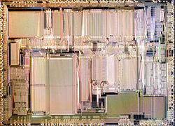
Intel's i960 (or 80960) is a RISC-based microprocessor design that became popular during the early 1990s as an embeddedmicrocontroller. It became a best-selling CPU in that segment, along with the competing AMD 29000.[3] In spite of its success, Intel stopped marketing the i960 in the late 1990s, as a result of a settlement with DEC whereby Intel received the rights to produce the StrongARM CPU. The processor continues to be used for a few military applications.
The i960 design was begun in response to the failure of Intel's iAPX 432 design of the early 1980s. The iAPX 432 was intended to directly support high-level languages that supported tagged, protected, garbage-collected memory—such as Ada and Lisp—in hardware. Because of its instruction-set complexity, its multi-chip implementation, and design flaws, the iAPX 432 was very slow in comparison to other processors of its time.
In 1984, Intel and Siemens started a joint project, ultimately called BiiN, to create a high-end, fault-tolerant, object-oriented computer system programmed entirely in Ada. Many of the original i432 team members joined this project, although a new lead architect, Glenford Myers, was brought in from IBM. The intended market for the BiiN systems was high-reliability-computer users such as banks, industrial systems, and nuclear power plants.
Intel's major contribution to the BiiN system was a new processor design, influenced by the protected-memory concepts from the i432. The new design was to include a number of features to improve performance and avoid problems that had led to the i432's downfall. The first 960 processors entered the final stages of design, known as taping-out, in October 1985 and were sent to manufacturing that month, with the first working chips arriving in late 1985 and early 1986.
The BiiN effort eventually failed, due to market forces, and the 960 was left without a use. Myers attempted to save the design by extracting several subsets of the full capability architecture created for the BiiN system. He tried to convince Intel management to market the i960 (then still known as the "P7") as a general-purpose processor, both in place of the Intel 80286 and i386 (which taped-out the same month as the first i960), as well as the emerging RISC market for Unix systems, including a pitch to Steve Jobs for use in the NeXT system. Myers was unsuccessful at convincing Intel management to support the i960 as a general-purpose or Unix processor, but the chip found a ready market in early high-performance 32-bit embedded systems.
The i960 family features four distinct architectures, designed for upward binary compatibility: [5]
Core architecture is a RISC-like core
Numerics architecture adds floating point
Protected architecture adds paged memory management, supervisor/user protection, string instructions, process scheduling, interprocess communication for the OS, and symmetric multiprocessing
Extended architecture adds object protection and interprocess communication for applications
In the initial release, the 80960KA supported the Core architecture, the 80960KB supported the Numerics architecture, the 80960MC supported the Protected architecture, and the 80960XA supported the Extended architecture.
To avoid the performance issues that plagued the i432, the central i960 instruction-set architecture was a RISC design. In the Extended architecture, the memory subsystem was 33-bits wide—to accommodate a 32-bit word and a "tag" bit to implement memory protection in hardware. In many ways, the i960 followed the original Berkeley RISC design, notably in its use of register windows, an implementation-specific number of caches for the per-subroutine registers that allowed for fast subroutine calls. The competing Stanford University design, MIPS, did not use this system, instead relying on the compiler to generate optimal subroutine call and return code. In common with most 32-bit designs, the i960 has a flat 32-bit memory space, with no memory segmentation, except for the Extended architecture, which could support up to 226 "objects", each up to 232 bytes in size.[6] The i960 architecture also anticipated a superscalar implementation, with instructions being simultaneously dispatched to more than one unit within the processor.
i960 variants
80960MC
The i960MC included all of the features of the original BiiN system; but these were simply not mentioned in the specifications, leading some[who?] to wonder why the i960MC was so large and had so many pins - 53 out of 132[7] - labeled "no connect". Later iterations of the i960, like the 80960Jx series, have a more typical number of "do no connect" and use more power and ground pins and have additional I/O pins instead.[8] However, these "no connect" pins are actually not connected internally and unrelated to the BiiN feature set - the silicon die inside does not have bond pads for them.[9]
The 80960MC contains an on-chip memory management unit and supports fault tolerant systems in conjunction with Intel's M82965 Bus Extension Unit as well. Both chips meets MIL-STD-883C standard. Both chips became available in the first quarter of 1989 with the price of US$2400 and US$1700 respectively. Extended temperature samples became available in August 1988 as well.[10]
It contains 32 32-bit registers, a 512 byte instruction cache, a stack frame cache, a high speed 32-bit multiplexed burst bus, and an interrupt controller.[11] It also has 256 interrupt vectors and 32 levels of interrupt priority.[10]
80960XA
The 80960XA is a military member of the i960 family, implementing the Extended architecture, a superset of the military 80960MC. It supports object-oriented programming with a 33rd tag bit in hardware, a Capability. It supports the Joint Industrial Avionics Working Group (JIAWG) 32-bit ISA standard.[5]
80960KA, 80960KB
A version of the RISC core without memory management or an FPU became the i960KA, and the RISC core with an FPU became the i960KB. The versions were, however, identical internally—only the labeling was different. This meant the CPUs were much larger than necessary for the "actually supported" feature sets, and as a result, more expensive to manufacture than they needed to be.
These processors contain more than 350,000 transistors. These processors can perform around 7.5 VAXMIPS. The 80960KB version is compatible with IEEE 754 standard and can perform up to 4MWIPS. Both processors are available in 16 and 20MHz using CHMOS-III technology. Both processors are packaged in 132-PGA. The 80960KA version is available for US$230 and the 80960KB version is available for US$390 in quantities of 100 respectively.[11]
The i960KA became successful as a low-cost 32-bit processor for the laser-printer market, as well as for early graphics terminals and other embedded applications. Its success paid for future generations, which were without the complex memory sub-system.
80960CA, 80960CF
The i960CA was announced in July 1989. It featured a newly designed superscalar RISC core and added an unusual addressable on-chip cache, but lacked an FPU and MMU, as it was intended for high-performance embedded applications. The i960CA is widely considered[12] to have been the first single-chip superscalar RISC implementation. The C-series included only one ALU, but could dispatch and execute an arithmetic instruction, a memory reference, and a branch instruction at the same time, and sustain two instructions per cycle under certain circumstances. The first versions released ran at 33MHz, and Intel promoted the chip as capable of 66 MIPS. The i960CA microarchitecture was designed in 1987–1988 and formally announced on September 12, 1989.
Later, in May 1992, came the i960CF, which included a larger instruction cache (4 KB instead of 1 KB) and added 1 KB of data cache, but was still without an FPU or MMU.
80960MX
The 80960MX is a superscalar implementation of the Extended architecture, executing up to three instructions per clock execution for sustained performance of 25 VAX MIPS.[13] It implemented the Joint Industrial Avionics Working Group (JIAWG) 32-bit ISA standard. It was originally packaged in a 348 lead ceramic pin grid array and later supplied as a bare die. The i960 MX supports object-oriented programming. A 33rd tag bit distinguished between a 32-bit data word and a 32-bit pointer to memory. This prohibited forged pointers to protected areas of memory.
80960Jx
The 80960Jx is a processor for embedded applications. It features a 32-bit multiplexed address/data bus, instruction and data cache, 1K on-chip RAM, interrupt controller, and two independent 32-bit timers. The 80960Jx's testability features included ONCE (on-circuit emulation) mode and boundary scan (JTAG).
80960HA, 80960HD, 80960HT
The 80960Hx processors offered upgraded performance from the Cx variants by offering clock multiplication, larger 16K instruction cache and 4k data cache, and a GMU (Guarded Memory Unit). The HD variant had an internal 2× clock multiplication while the HT version has a 3x clock multiplication, allowing increased performance without external bus speed changes.
80960VH
Announced in October 1998, the i960VH Embedded-PCI processor featured a 32-bit 33MHz PCI bus and 100MHz i960JT processor core. The core also featured 16KB of instruction cache, 4KB of data cache, and 1KB of built-in RAM. Other core features included two 32-bit timers, programmable interrupt controller, I²C interface, and a two-channel DMA controller.
80960Rx
The 80960Rx processors were labeled as I/O Processors and included an implementation of the PCI Bus (2.1 or 2.2 depending on the variant) as well as a 80960Jx core. These could be used on motherboards to implement on-board PCI device as well as on PCI expansion cards. The RM/RN/RS variants used a JT core with a 3x bus to core multiplication to achieve 100MHz internal clock speeds, while the RD variant used a JF core with 2× multiplication to achieve 66MHz. The RP variant had a JF core that ran at the 33MHz bus speed.
Intel attempted to bolster the i960 in the I/O device controller market with the I2O standard, but this had little success and the design work was eventually ended. By the mid-1990s its price/performance ratio had fallen behind competing chips of more recent design, and Intel never produced a reduced-power-consumption version that could be used in battery-powered systems.
In 1990, the i960 team was redirected to be the "second team" working in parallel on future i386 implementations—specifically the P6 processor, which later became the Pentium Pro. The i960 project was given to another smaller development team, essentially ensuring the end of its developmental life.
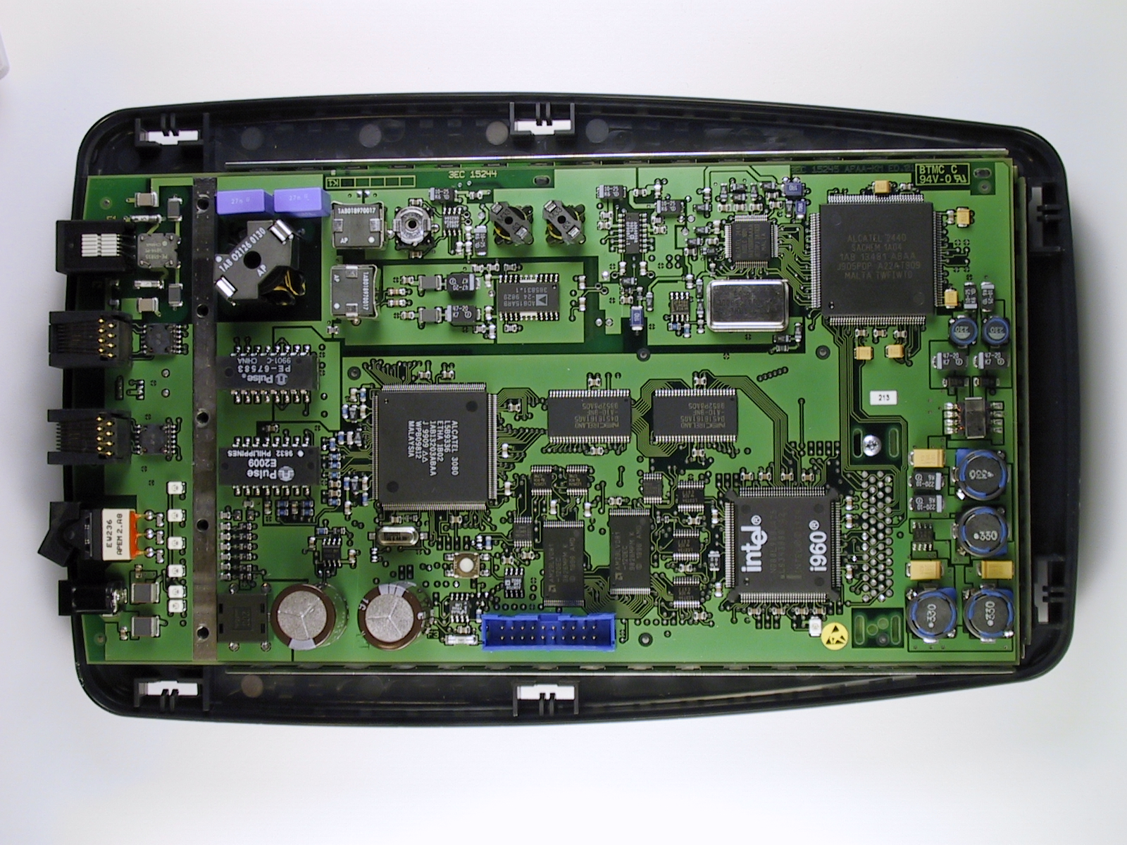
Some i960 I/O processors, such as the 80303, include a built-in hardware XOR engine for RAID algorithms.[14] They are used as controllers for higher-end, RAID-capable, SCSI-disk-array, host-adapter cards as well as Digital Equipment/Compaq/HP's high-end SCSI and DSSI, and eventually Fibre Channel HSx-series, standalone RAID controllers.[15][16]
An i960RS chip also powers Adaptec's AAR-2400A controller, which uses four commodity parallel ATA drives to build an affordable RAID-5 protected fault-tolerant storage system for small PC servers and workstations.
The i960 architecture is also used in slot machines. Currently, they are found in IGT's Stepper S2000 family and i960 video family. It was also used as the main CPU of Sega's famous Model 2 series of arcade boards.
The Indian Air Force's HAL Tejas light combat aircraft's MMR (multi-mode radar) is said to use the i960. The HAL Tejas was introduced into service in 2015.
Some SATA RAID controllers use Intel's 80303 IOP (Intelligent I/O Processor), which integrates a PCI-to-PCI bridge, memory controller, and a 80960JT-100 CPU core.
↑ Shirriff, Ken (July 1, 2023). "The complex history of the Intel i960 RISC processor". Retrieved July 1, 2023. The original i960 chips (KA/KB/MC/XA) have a large number of pins that are not connected (marked NC on the datasheet) [...] checking the datasheets shows that all four chips have the same pinout; there are no pins connected only in the more advanced versions. Second, looking at the packaged chip (below) explains why so many pins are unconnected: much of the chip has no bond pads, so there is nothing to connect the pins to.
1 2 Lewnes, Ann, "Intel's 80960 & 80376 Standouts in the 32-Bit Crowd", Intel Corporation, Microcomputer Solutions, July/August 1988, page 2
1 2 Ormsby, Jon, Editor, "New Product Focus: Components: Intel Enters The World Of 32-Bit Embedded Control", Intel Corporation, Microcomputer Solutions, May/June 1988, page 9
↑ Shen, John Paul; Lipasti, Mikko H. (2003). Modern Processor Design: Fundamentals of Superscalar Processors (Betaed.). McGraw Hill. p.328. ISBN0-07-282968-0.
↑ "i960 MX Processor". Military and Special Products Handbook. Intel. 1993. pp.11-40 to 11-89.
This page is based on this Wikipedia article Text is available under the CC BY-SA 4.0 license; additional terms may apply. Images, videos and audio are available under their respective licenses.


