July15,1999;26 years ago(1999-07-15) (orders and shipments)[1][bettersourceneeded] December31,2001;23 years ago(2001-12-31) (discontinuation and end of life)[2]
The Pentium (also referred to as the i586 or P5 Pentium) is a microprocessor introduced by Intel on March 22, 1993. It is the first CPU using the Pentium brand.[5][6] Considered the fifth generation in the x86 (8086) compatible line of processors,[7] succeeding the i486, its implementation and microarchitecture was internally called P5.
Like the Intel i486, the Pentium is instruction set compatible with the 32-bit i386. It uses a very similar microarchitecture to the i486, but was extended enough to implement a dual integer pipeline design, as well as a more advanced floating-point unit (FPU) that was noted to be ten times faster than its predecessor.[8]
The Pentium was succeeded by the Pentium Pro in November 1995. In October 1996, the Pentium MMX[9] was introduced, complementing the same basic microarchitecture of the original Pentium with the MMX instruction set, larger caches, and some other enhancements. Intel discontinued the original Pentium (P5) processors, which were sold as a lower-cost option after the Pentium II's release in 1997, on December 31, 2001. This coincided with Microsoft ending support for classic versions of Windows such as Windows 95. The Pentium line was gradually replaced by the Celeron processor, which also took over the role of the 80486 brand.[1][2]
Overview
The P5 Pentium is the first superscalarx86 processor, meaning it was often able to execute two instructions at the same time.[10] Some techniques used to implement this were based on the earlier superscalar Intel i960 CA (1989), while other details were invented exclusively for the P5 design. Large parts were also copied from the i386 or i486, especially the strategies used to cope with the complicated x86 encodings in a pipelined fashion.[11] Just like the i486, the Pentium used both an optimized microcode system and RISC-like techniques, depending on the particular instruction, or part of instruction. The dual integer pipeline design is something that had been argued being impossible to implement for a CISC instruction set, by certain academics and RISC competitors.[who?]
Other central features include a redesigned and significantly faster floating-point unit, a wide 64-bit burst-mode data bus (external as well as internal), separate code and data caches, and many other techniques and features to enhance performance. It contains 256-bit internal data buses and write-back caches.[12] It does contain System Management Mode that has been implemented since the Intel's SL architecture.[13]
The 66-MHz Pentium processor operates at 112 V1.1 Dhrystone MIPS and has SPECint92 rating of 64.5, a SPECfp92 rating of 56.9 and an iCOMP index rating of 567. The performance difference between 60- and 66-MHz version is about 10%.[14]
The P5 also has better support for multiprocessing compared to the i486, and is the first x86 CPU with hardware support for it similar to IBM mainframe computers. Intel worked with IBM to define this ability and also designed it into the P5 microarchitecture. This ability was absent in prior x86 generations and x86 processors from competitors.
In order to employ the dual pipelines at their full potential, certain compilers were optimized to better exploit instruction level parallelism, although not all applications would substantially gain from being recompiled. The faster FPU always enhanced floating point performance significantly though, compared to the i486 or i387. Intel spent resources working with development tool vendors, ISVs and operating system (OS) companies to optimize their products.
The name "Pentium" is originally derived from the Greek word pente (πέντε), meaning "five", a reference to the prior numeric naming convention of Intel's 80x86 processors (8086–80486), with the Latin ending -ium since the processor would otherwise have been named 80586 using that convention.
Development
The P5 microarchitecture was designed by the same Santa Clara team which designed the 386 and 486.[15] Design work started in June 1989;[16]:88 the team decided to use a superscalar RISC architecture which would be a convergence of RISC and CISC technology,[17] with on-chip cache, floating-point, and branch prediction.[18]Vinod Dham then the Vice President of the Microprocessor Product Group and General Manager of Microprocessor Division 5/7 had the concept using this RISC technology into the existing x86 architecture that could compete from the other market.[19] Their performance target could boost FPU by three times and five time over the existing Intel486 CPU.[20] The preliminary design was first successfully simulated in 1990, followed by the laying-out of the design. By this time, the team had several dozen engineers. It took some 100 million clock cycles of pre-silicon verification test which includes major operating systems and many application were booted and running. They had to use the Quickturn Systems Inc. software to run pre-silicon simulation program which was 30,000 times quicker than the previous technique method available.[21] By late 1990, they found that the planned feature could not fit into the die, they had to redesign the circuit feature that would slim down in order to fit what the intended design in place without sacrificing the performance. In spring of 1991, the die went another slimming procedure until Dham was happy with the size and its feature without affecting the performance. A group of engineers ran hundreds of tests to validate the designed features and ran 5000 different variables to validate its design. Out of the 14 circuit boards in collection and cables, they only found few bugs using every operating system they have it on hand including in development were used.[22] By February 1992, the design was taped out in process which was completed by April 1992, at which point beta-testing began.[23][24] The next few months the design was sent to the Intel's Mask Operation which it translate to mask layout for the Oregon's Fab 5 to be processed.[25] By mid-1992, the P5 team had 200 engineers.[16]:89 Intel at first planned to demonstrate the P5 in June 1992 at the trade show PC Expo, and to formally announce the processor in September 1992,[26] but design problems forced the demo to be cancelled, and the official introduction of the chip was delayed until the spring of 1993.[27][28] The first computer systems featuring the Pentium appeared in the summer of 1993, the first being Advanced Logic Research and their Evolution V workstation, released in the first week of July 1993.[29][30][31]
John H. Crawford, chief architect of the original 386, co-managed the design of the P5,[32] along with Donald Alpert, who managed the architectural team. Dror Avnon managed the design of the FPU.[33]Vinod K. Dham was general manager of the P5 group.[16]:90
Intel used the Pentium name instead of 586, because in 1991, it had lost a trademark dispute over the "386" trademark, when a judge ruled that the number was generic. The company hired Lexicon Branding to come up with a new, non-numeric name.[36]
Improvements over the i486
The P5 microarchitecture brings several important advances over the prior i486 architecture.
Performance:
Superscalar architecture – The Pentium has two datapaths (pipelines) that allow it to complete two instructions per clock cycle in many cases. The main pipe (U) can handle any instruction, while the other (V) can handle the most common simple instructions. The first instruction goes to the U pipeline, then the next instruction goes to the V pipeline. Both pipelines contain their own ALU, address generation circuitry and interface to the data cache.[37] Some[who?]reduced instruction set computer (RISC) proponents had argued that the "complicated" x86 instruction set would probably never be implemented by a tightly pipelined microarchitecture, much less by a dual-pipeline design. The 486 and the Pentium demonstrated that this was indeed possible and feasible.
64-bit burst-mode external databus doubles the amount of information possible to read or write on each memory access and therefore allows the Pentium to load its code cache faster than the 80486; it also allows faster access and storage of 64-bit and 80-bit x87FPU data. Internally, this CPU process the data at 32 bits wide. The external data to the memory is 64 bits wide which it doubles the amount of data being transferred in one bus cycle. It includes several types of bus cycles which includes burst mode that loads 256-bit portions of data into its data cache in one bus cycle as well. This data width can transfer data up to 528 Mbytes per second from and to the memory. This rate has increased three-fold over its peak transfer rate of the 50-MHz Intel486 DX CPU.[38]
Separation of code and data in both 8-Kbyte on-chip caches[39] lessens the fetch and operand read/write conflicts compared to the 486. One set is for the instruction, and the other set is for the data.[40] To reduce access time and implementation cost, both of them are 2-way associative, instead of the single 4-way cache of the 486. Using pair of cache's 32-byte lines to match up the 64-bit width with a four-chuck burst length. This cache management conforms to the MESI cache-consistency protocol.[41] A related enhancement in the Pentium is the ability to read a contiguous block from the code cache even when it is split between two cache lines (at least 17 bytes in worst case).
Much faster floating-point unit. This component incorporates an eight-stage pipeline that executes at least one floating-point operation every clock cycle. The first four stages of this pipeline use the integer part, and the final four stages are a two-stage floating-point execution, rounding and writing of the result to the register file and the error reporting. This unit also has new algorithms that increase the speed of these common operation by the factor of three time than the predecessor CPU.[42] Some instructions showed an enormous improvement, most notably FMUL, with up to 15 times higher throughput than in the 80486 FPU. The Pentium is also able to execute a FXCH ST(x) instruction in parallel with an ordinary (arithmetical or load/store) FPU instruction.
Four-input address adders enables the Pentium to further reduce the address calculation latency compared to the 80486. The Pentium can calculate full addressing modes with segment-base + base-register + scaled register + immediate offset in a single cycle; the 486 has a three-input address adder only, and must therefore divide such calculations between two cycles.
The microcode can employ both pipelines to enable auto-repeating instructions such as REP MOVSW perform one iteration every clock cycle, while the 80486 needed three clocks per iteration (and the earliest x86 chips significantly more than the 486). Also, optimization of the access to the first microcode words during the decode stages helps in making several frequent instructions execute significantly more quickly, especially in their most common forms and in typical cases. Some examples are (486→Pentium, in clock cycles): CALL (3→1), RET (5→2), shifts/rotates (2–3→1).
A faster, fully hardware-based multiplier makes instructions such as MUL and IMUL several times faster (and more predictable) than in the 80486; the execution time is reduced from 13 to 42 clock cycles down to 10–11 for 32-bit operands.
Dynamic Branch Prediction using the branch target buffer method that contains a small cache block. Using the Sieve of Eratosthenes benchmark method requires six clock cycles to execute on the Intel486 CPU down to two clock cycles in this CPU.[43]
Other features:
Enhanced debug features with the introduction of the Processor-based debug port (see Pentium Processor Debugging in the Developers Manual, Vol 1).
Enhanced self-test features like the L1 cache parity check (see Cache Structure in the Developers Manual, Vol 1). Other built-in features include an IEEE 1149.1 compliant access architecture for testing external connectivity to the CPU and a probe mode to access the software visible register and the processor state.[44]
New instructions: CPUID, CMPXCHG8B, RDTSC, RDMSR, WRMSR, RSM.
Test registers TR0–TR7 and MOV instructions for access to them were eliminated.
The later Pentium MMX also added the MMX instruction set, a basic integer single instruction, multiple data (SIMD) instruction set extension marketed for use in multimedia applications. MMX could not be used simultaneously with the x87 FPU instructions because the registers were reused (to allow fast context switches). More important enhancements were the doubling of the instruction and data cache sizes and a few microarchitectural changes for better performance.
The Pentium was designed to execute over 100million instructions per second (MIPS),[45] and the 75MHz model was able to reach 126.5 MIPS in certain benchmarks.[46] The Pentium architecture typically offered just under twice the performance of a 486 processor per clock cycle in common benchmarks. The fastest 80486 parts (with slightly improved microarchitecture and 100MHz operation) were almost as powerful as the first-generation Pentiums, and the AMDAm5x86, which despite its name is actually a 486-class CPU, was roughly equal to the Pentium 75 regarding pure ALU performance.
Errata
The early versions of 60–66MHz P5 Pentiums had a problem in the floating-point unit that resulted in incorrect (but predictable) results from some division operations. This flaw, discovered in 1994 by professor Thomas Nicely at Lynchburg College, Virginia, became widely known as the Pentium FDIV bug and caused embarrassment for Intel, which created an exchange program to replace the faulty processors.
In 1997, another erratum was discovered that could allow a malicious program to crash a system without any special privileges, the "F00F bug". All P5 series processors were affected and no fixed steppings were ever released, however contemporary operating systems were patched with workarounds to prevent crashes.
Cores and steppings
The Pentium was Intel's primary microprocessor for personal computers during the mid-1990s. The original design was reimplemented in newer processes and new features were added to maintain its competitiveness, and to address specific markets such as portable computers. As a result, there were several variants of the P5 microarchitecture.
P5
Intel Pentium microarchitecture
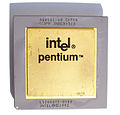
The first Pentium microprocessor core was code-named "P5". Its product code was 80501 (80500 for the earliest steppings Q0399). There were two versions, specified to operate at 60MHz and 66MHz respectively, using Socket 4. This first implementation of the Pentium was released using a 273-pin PGA form factor and ran on a 5 V power supply. (descended from the usual transistor-transistor logic (TTL) compatibility requirements). It contained 3.1 million transistors and measured 16.7mm by 17.6mm for an area of 293.92mm2.[47] It was fabricated in a 800nm three-layer metal bipolar complementary metal–oxide–semiconductor (BiCMOS) process.[48][49] The 5-volt design resulted in relatively high energy consumption for its operating frequency when compared to the directly following models.
P54C
Intel Pentium P54C die shot
The P5 was followed by the P54C (80502) in 1994, with versions specified to operate at 75, 90, or 100MHz using a 3.3 volt power supply. Marking the switch to Socket 5, this was the first Pentium processor to operate at 3.3 volts, reducing energy consumption, but necessitating voltage regulation on mainboards. As with higher-clocked 486 processors, an internal clock multiplier was employed from here on to let the internal circuitry work at a higher frequency than the external address and data buses, as it is more complicated and cumbersome to increase the external frequency, due to physical constraints. It also allowed two-way multiprocessing, and had an integrated local APIC and new power management features. It was fabricated in a BiCMOS process which has been described as both 500nm and 600 nm due to differing definitions.[50]
P54CQS
The P54C was followed by the P54CQS in early 1995, which operated at 120MHz. It was fabricated in a 350nm BiCMOS process and was the first commercial microprocessor to be fabricated in a 350nm process.[50] Its transistor count is identical to the P54C and, despite the newer process, it had an identical die area as well. The chip was connected to the package using wire bonding, which only allows connections along the edges of the chip. A smaller chip would have required a redesign of the package, as there is a limit on the length of the wires and the edges of the chip would be further away from the pads on the package. The solution was to keep the chip the same size, retain the existing pad-ring, and only reduce the size of the Pentium's logic circuitry to enable it to achieve higher clock frequencies.[50]
P54CS
The P54CQS was quickly followed by the P54CS, which operated at 133, 150, 166 and 200MHz, and introduced Socket 7. It contained 3.3 million transistors, measured 90mm2 and was fabricated in a 350nm BiCMOS process with four levels of interconnect.
The P24T Pentium OverDrive for 486 systems were released in 1995, which were based on 3.3V 600nm versions using a 63 or 83MHz clock. Since these used Socket 2/3, some modifications had to be made to compensate for the 32-bit data bus and slower on-board L2 cache of 486 motherboards. They were therefore equipped with a 32KB L1 cache (double that of pre-P55C Pentium CPUs).
P55C
Intel Pentium MMX microarchitecturePentium MMX 166MHz without cover
The P55C (or 80503) was developed by Intel's Research & Development Center in Haifa, Israel. It was sold as Pentium with MMX Technology (usually just called Pentium MMX); although it was based on the P5 core, it featured a new set of 57 "MMX" instructions intended to improve performance on multimedia tasks, such as encoding and decoding digital media data. The Pentium MMX line was introduced on October 22, 1996, and released in January 1997.[51]
The new instructions worked on new data types: 64-bit packed vectors of either eight 8-bit integers, four 16-bit integers, two 32-bit integers, or one 64-bit integer. So, for example, the PADDUSB (Packed ADD Unsigned Saturated Byte) instruction adds two vectors, each containing eight 8-bit unsigned integers together, elementwise; each addition that would overflowsaturates, yielding 255, the maximal unsigned value that can be represented in a byte. These rather specialized instructions generally require special coding by the programmer for them to be used.[citation needed]
Other changes to the core include a 6-stage pipeline (vs. 5 on P5) with a return stack (first done on Cyrix 6x86) and better parallelism, an improved instruction decoder, 16KB L1 data cache + 16KB L1 instruction cache with Both 4-way associativity (vs. 8KB L1 Data/instruction with 2-way on P5), 4 write buffers that could now be used by either pipeline (vs. one corresponding to each pipeline on P5) and an improved branch predictor taken from the Pentium Pro,[52][53] with a 512-entry buffer (vs. 256 on P5).[54]
It contained 4.5 million transistors and had an area of 140mm2. It was fabricated in a 280nm CMOS process with the same metal pitches as the previous 350nm BiCMOS process, so Intel described it as "350nm" because of its similar transistor density.[55] The process has four levels of interconnect.[55]
While the P55C remained compatible with Socket 7, the voltage requirements for powering the chip differ from the standard Socket 7 specifications. Most motherboards manufactured for Socket 7 before the establishment of the P55C standard are not compliant with the dual voltage rail required for proper operation of this CPU (2.8 volt core voltage, 3.3 volt input/output (I/O) voltage). Intel addressed the issue with OverDrive upgrade kits that featured an interposer with its own voltage regulation.
Tillamook
Pentium MMX notebook CPUs used a mobile module that held the CPU. This module was a printed circuit board (PCB) with the CPU directly attached to it in a smaller form factor. The module snapped to the notebook motherboard, and typically a heat spreader was installed and made contact with the module. However, with the 250nm Tillamook Mobile Pentium MMX (named after a city in Oregon), the module also held the 430TX chipset along with the system's 512 KB static random-access memory (SRAM) cache memory.
After the introduction of the Pentium, competitors such as NexGen,[56] AMD, Cyrix, and Texas Instruments announced Pentium-compatible processors in 1994.[57]CIO magazine identified NexGen's Nx586 as the first Pentium-compatible CPU,[58] while PC Magazine described the Cyrix 6x86 as the first. These were followed by the AMD K5, which was delayed due to design difficulties. AMD later bought NexGen to help design the AMD K6, and Cyrix was bought by National Semiconductor.[59] Later processors from AMD and Intel retain compatibility with the original Pentium.
The Pentium Timeline ProjectArchived December 23, 2021, at the Wayback Machine The Pentium Timeline Project maps oldest and youngest chip known of every s-spec made. Data are shown in an interactive timeline.
This page is based on this Wikipedia article Text is available under the CC BY-SA 4.0 license; additional terms may apply. Images, videos and audio are available under their respective licenses.