"4004" redirects here. For 4004 BC as the putative beginning of the world, see Ussher chronology. For 4004 BC in other contexts, see 5th millennium BC.
The Intel 4004,[2] released by the Intel Corporation on November 15, 1971,[3] was the first in a long line of Intel central processing units (CPUs). Priced at US$60(equivalent to $466 in 2024), the chip marked both a technological and economic milestone in computing.
The 4-bit 4004 CPU was the first significant commercial example of large-scale integration, using the abilities of the MOS silicon gate technology (SGT) to integrate the CPU into a single chip. Compared to the existing technology, SGT enabled twice the transistor density and five times the operating speed, making future single-chip CPUs feasible. The MCS-4 chipset design, of which the 4004 was a part, served as a model on how to use SGT for complex logic and memory circuits, accelerating the adoption of SGT by the world's semiconductor industry.
The project originated in 1969 when Busicom Corp. commissioned Intel to design a family of seven chips for electronic calculators, including a three-chip CPU.[4] Busicom initially envisioned using shift registers for data storage and ROM for instructions. Intel engineer Marcian Hoff proposed a simpler architecture based on data stored on RAM, making a single-chip CPU possible. Design work, led by Federico Faggin with contributions from Masatoshi Shima, began in April 1970. The first fully operational 4004 was delivered in March 1971 for Busicom's 141-PF printing calculator prototype, now housed at the Computer History Museum.[5] General sales began in July 1971.
Faggin, who had developed SGT at Fairchild Semiconductor and used it to create the Fairchild 3708, the first commercially produced SGT integrated circuit (IC), used SGT, a method of using poly-silicon instead of metal, at Intel to achieve the integration required for the 4004. Additionally, he developed the "bootstrap load," previously considered unfeasible with silicon gate technology, and the "buried contact," which enabled silicon gates to connect directly to the transistor's source and drain without the use of metal. Together, these innovations doubled the circuit density, and thus halved cost, allowing a single chip to contain 2,300 transistors and run five times faster than designs using the previous MOS technology with aluminum gates.
The 4004's architecture laid the foundation for subsequent Intel processors, including the improved Intel 4040, released in 1974, and the 8-bit Intel 8008 and 8080.
History
Original concept
In April 1969, Busicom approached Intel and asked them to produce a chip set to handle the operations for an electronic calculator.[4] The partnership was facilitated in part by Sharp engineer Tadashi Sasaki, who had been dreaming for decades of miniaturizing computers to the point where they could fit into a pocket. Sasaki monitored the trend of increasing integrated circuit complexity throughout the 1960s, and calculated in 1968 that by 1970 it should be affordable to build a calculator out of just two chips. Sasaki discussed his ideas for low-cost, low-chip-count processor designs with his college classmate Yoshio Kojima, who was president of Busicom, as well as with Robert Noyce of Intel.[6] Busicom was interested in building a lower-cost competitor to the 1965 Olivetti Programma 101, one of the world's first tabletop programmable calculators.[7][8] The key difference was that the Busicom design would use integrated circuits to replace the printed circuit boards filled with individual components, and solid-state shift registers for memory instead of the costly magnetostriction wire in the 101. Busicom also realized that they could launch a general-purpose processor in a low-end desktop printing calculator, and then use the same design for other equipment like cash registers and automatic teller machines. The company had already produced a calculator using TTLsmall-scale integration logic ICs and were interested in having Intel reduce the chip count using Intel's medium-scale integration (MSI) techniques.[9]
Intel assigned the recently hired Marcian Hoff, employee number 12, to act as the liaison between the two companies. In late June, three engineers from Busicom, Masatoshi Shima and his colleagues Masuda and Takayama, traveled to Intel to introduce the design. Although he had only been assigned to liaise with the engineers, Hoff began studying the concept. Their initial proposal had seven ICs: program control, arithmetic unit (ALU), timing, program ROM, shift registers for temporary memory, printer controller and input/output control.[10]
Hoff became concerned that the number of chips and the required interconnections between them would make Busicom's price goals impossible to meet. Combining the chips would reduce the complexity and cost. He was also concerned that the still-small Intel would not have enough design staff to make seven separate chips at the same time. He raised these concerns with upper management, and Bob Noyce, the CEO, told Hoff he would support a different approach if it seemed feasible.[10]
Simplified design
Chip layout from the development phase of the Intel 4004
A key concept in the Busicom design was that the program control and ALU were not aimed specifically at the calculator market, it was the program in ROM that turned it into a calculator. The original idea was that the company could use the same chips with different amounts of shift-register RAM and program ROM to produce a range of calculating machines. Hoff was struck by how closely the Busicom's instruction set architecture matched that of general-purpose computers. He began to consider whether a truly general-purpose processor could be made cheaply enough to be used in a calculator.[11] When later asked where he got the ideas for the architecture of the first microprocessor, Hoff related that Plessey, "a British tractor company",[12] had donated a minicomputer to Stanford, and he had "played with it some" while he was there.
Another development that made this design practical was Intel's work on the earliest dynamic RAM (DRAM) chips. Shift registers at that time were among the only low-cost read and write memory devices. However, shift register memory is not suited for random access, as each access must wait for the desired bit to flow through the chain. DRAM, on the other hand, can be accessed randomly, and the three-transistor DRAM cell saves silicon area compared to the six-transistor shift-register cell.[11]
Finally, Hoff noticed that much of the complexity of the program control chip was due to every instruction being implemented separately. He suggested that the chip instead support subroutine calls and instructions be implemented as subroutines where possible. The application naturally suggested a 4-bit design, as this allowed for direct manipulation of binary-coded decimal (BCD) values used by calculators. Hoff worked on the overall design concept through July and August 1969 but found that the Busicom executives seemed uninterested in his proposal.[11] Intel had to work smarter so Busicom would accept their proposal for the 141-PF calculator. They began to conceptualize a general purpose microprocessor that could be given instructions and return their results, as well as be able to merge all of the CPU functions of a computer.[13] Later in fall of that year, Intel's engineers proposed a new design of just four chips, including one that could be programmed for use; the programmable chip would end up becoming the 4004 microprocessor.[4]
Mazor joins
Unknown to Hoff, the Busicom team were extremely interested in his proposal. However, there were a number of specific issues that they were concerned about. One key issue was that certain routines like decimal adjust and keyboard handling would use large amounts of ROM space if implemented as subroutines. Another was that the design did not feature any sort of interrupt, so dealing with real-time events would be difficult. Finally, storing the numbers as 4-bit BCD would require additional memory to store the sign and decimal place.[14]
In September 1969, Stanley Mazor joined Intel from Fairchild. Hoff and Mazor quickly came up with solutions to the Busicom concerns. To address the complexity of the subroutines, originally solved in Busicom's design using one-byte macroinstructions and complex decoder circuitry, Mazor developed a 20-byte long interpreter that executed the same macroinstructions. Shima suggested adding a new interrupt that would be triggered by a pin so that the keyboard could be interrupt driven. He also modified the Branch Back (return from subroutine) instruction to clear the accumulator.[15]
To reach the price goals, it was important that the chip be as small as possible and use the fewest number of leads. As data was 4bits and the address space was 12bits (4096bytes), there was no way direct access could be arranged with anything fewer than about 24pins. This was not small enough, so the design would use a 16-pin dual in-line package (DIP) layout and use multiplexing of a single set of 4 lines. This meant specifying which address in ROM to access required three clock cycles, and another two to read it from memory. Running at 1MHz it would perform math on the BCD values at about 80microseconds per digit.[16]
The result of the discussions between Intel and Busicom was an architecture that reduced the 7-chip Busicom design to a 4-chip Intel proposal composed of CPU, ROM, RAM and I/O (input-output) devices. The proposal was presented to a visiting team of Busicom executives in October 1969. They agreed that the new concept was superior and gave Intel the go-ahead to begin development. Hoff was upset to learn that the contract assigned all rights to the design to Busicom, in spite of it being designed entirely within Intel. The team then left for Japan, but Shima remained in California until December, developing many of the subroutines.[16]
Faggin joins
Neither Hoff nor Mazor, who worked in the Applications Research group, had experience designing the actual silicon, and the design group was already overworked with the development of memory devices. In April 1970, Leslie Vadász, who ran the MOS design group, hired Federico Faggin from Fairchild Semiconductor to take over the project.[17] Faggin had already made a name for himself by leading the entire development of the MOS silicon gate technology and the design of the first commercial integrated circuit (IC) made with it. The new technology was going to change the entire semiconductor market.
Integrated circuits consist of a number of individual components like transistors and resistors that are produced by mixing the underlying silicon with "dopants". This is normally accomplished by heating the chip in the presence of a chemical gas, which diffuses into the surface. Previously, the individual components were connected together to make a circuit using aluminum wires deposited on the surface. As aluminum melts at 600 degrees and silicon at 1000, the traces typically had to be deposited as the last step, which often complicated the production cycle.
In 1967, Bell Labs released a paper about making MOS transistors with self-aligned gates made of silicon rather than metal. These devices, however, were a proof-of-concept and could not be used to make ICs. Faggin and Tom Klein had taken what was a curiosity and developed the entire process technology needed to fabricate reliable ICs. Faggin also designed and produced the Fairchild 3708,[18] the first IC made with SGT, first sold at the end of 1968, and featured on the cover of Electronics in September 1969.[19][17] The silicon gate technology also reduced the leakage current by more than 100 times, making possible sophisticated dynamic circuits like DRAMs (dynamic random access memories). Also, the highly doped silicon used for the gates could be used for the interconnections, and this greatly improved the circuit density of random-logic ICs like microprocessors.
This technique meant the interconnections could be performed at any time in the process. More importantly, the wiring was deposited using the same equipment that made the rest of the components. This meant that the slight differences in layout between different machine types was eliminated. Previously the interconnects had to be much larger than required in order to ensure the aluminum touched the silicon components which would be offset due to inaccuracies in the machinery. With this issue eliminated, the circuits could be placed much closer together, immediately doubling the density of the components and reducing their cost by the same amount. Additionally, the aluminum wiring acted as parasitic capacitors which limited the signal speed; without these parasitics the chips could run at faster speeds.[20][21]
At Intel, Faggin began designing the new processor using this self-aligned gate process. Only days after Faggin joined Intel, Shima arrived from Japan. He was disappointed to learn that the project had stalled since he'd left in December, and expressed concern his original schedule was now impossible. Faggin responded by working well into the night every day, and Shima stayed on for another six months to help. Faggin himself immersed himself in workweeks that spanned 70 to 80 hours.[22] Additional advances were needed to reach the required circuit density. One of these advances was the use of "buried contacts"[23][24] to connect the wires directly to the components. Another was figuring out how to make adding "bootstrap loads" with silicon gate as part of one of the masking steps,[25] eliminating one step from the processing.[17] Without these two innovations by Faggin, Hoff's architecture could not have been realized in a single chip.
Into production
Intel 4004 CPU and associated chips on the circuit board from a Busicom calculator
Intel's chip-naming scheme at that time used a four-digit number for each component. The first digit indicated the process technology used, the second digit indicated the generic function, and the last two digits specified the sequential number in the development of that component type. Using this convention, the chips would have been known as the 1302, 1105, 1507, and 1202. Faggin felt this would obscure the fact that they formed a coherent set, and decided to name them as the "4000 family".[26] The four chips were the following:
the Intel 4001, a 256-byte 4-bit ROM;
the Intel 4002, DRAM with four 20-nibble registers (total size 40 bytes);
the Intel 4003, an I/O chip comprising a 10-bit static shift register with serial and parallel outputs; and
the Intel 4004 CPU.
A fully expanded system could support 16 Intel 4001s for a total of 4kB of ROM, 16 Intel 4002s for a total of 1,280 nibbles (640 bytes) of RAM, and an unlimited number of 4003s. The 4003s were connected to programmable input and output pins on the 4001 and to output pins on the 4002, not directly to the CPU.[10]
With the design complete, Shima returned to Japan to begin building a prototype of the calculator. The first wafers of the 4001 were processed in October 1970,[17] followed by the 4003 and 4002 in November. The 4002 proved to have a minor problem that was easily corrected. The first 4004s arrived at the end of December, and were completely non-functional. Probing the chip, Faggin found that the buried-contact fabrication step had been left out. A second run was fabricated in January 1971 and the 4004 worked as expected except for two minor problems.
Faggin was sending samples of these chips to Shima as they arrived in February 1971.[4] In April of that year, they learned the calculator prototype was operational. Later that month Shima sent Intel the final masks for the 4001 ROMs, the design was now complete. It consisted of one 4004, two 4002, three 4003, and four 4001 chips. An additional 4001 supplied the optional square root function. One final change was added after Faggin found a problem in the 4001 and 4002 that occurred only when the chips were hot. Adding a new register decoder circuit in both solved the issue. Quantity production began in August 1971.[27]
Marketing the 4004
Intel 4004 advertisement in Electronic News magazine from 1971
During a call to Shima, Faggin learned that Busicom was in financial difficulty and would likely fail if the chip price was not reduced. Faggin then convinced Noyce to lower the price in exchange for releasing Intel from the exclusivity agreement. In May 1971, Busicom agreed to this, on the condition that it not be used for any other calculator project and that Intel would repay their $60,000 development costs.[27] With this change of marketing focus name of the chip family name was changed to MCS-4, short for Micro Computer System, 4-bit.[26]
Intel management was skeptical that their sales team could explain the product to their customers. As Intel was now successful in the memory market, they were concerned the 4004 might confuse the market and were hesitant to advertise it.[27] They feared current Intel customers might view the new product as competition, purchasing memory from competitors instead.[28] Hoff and Mazor were also concerned that the design's limitations would make it less interesting to users who were accustomed to the new 16-bit minicomputers entering the market at that time.[29]
This all changed in the summer of 1971, when Ed Gelbach, formerly of Texas Instruments, took over the marketing department and immediately began plans to publicly announce the product.[29] This took place in the November 1971 when Intel ran ads "Announcing a new era of integrated electronics,"[30] first appearing in the November 15 edition of Electronic News.[31]
The 8008
The 4004 became the first commercial microprocessor available for general use.[a] This was almost not the case.[29]
In December 1969, Intel was approached by Computer Terminal Corporation (CTC) to produce a custom bipolar memory chip for a computer terminal they were designing, the Datapoint 2200. Mazor and Hoff considered their CPU design and concluded it was not much more complicated than the 4004, and that it could be implemented as a single-chip 8-bit CPU.[16] A few weeks before they hired Faggin, in March 1970 Intel hired Hal Feeney to design the Intel 8008, at that time called the 1201, following Intel's naming convention. However, CTC decided to initially proceed with a conventional TTL implementation of their CPU and the project was lowered in priority. Feeney was assigned to other projects and ultimately ended up helping Faggin with testing the 4000 family chips.[32]
In January 1971, Feeney was reassigned back to the 1201 under Faggin's supervision and production chips were available in March 1972. In May, Hoff and Mazor went on a speaking tour to introduce the two CPU designs around the USA. The tradeoffs between the two designs were that with the 4004 and its memory and I/O chips it was much easier to build a complete computer system while the 8008 was more flexible, had a larger 16kB address space, and offered more instructions. A significant difference is that while a minimal 4004 system could be built using only two chips, one 4004 and one 4001 (256-byte ROM), the 8008 would require at least 20 additional TTL components for interfacing with memory and I/O functions.[32]
The two designs found themselves being used in different roles. The 4004 was used where the cost of implementation was the major concern, and became widely used in embedded controllers for applications like microwave ovens or traffic lights and similar roles. The 8008 instead found itself mostly used in user-programmable applications, such as computer terminals, microcomputers and similar roles. This split in functionality remains to this day, with the former being known as a microcontroller.[32]
Description
National Semiconductor was a second-source manufacturer of the 4004, under their part number INS4004.
The Intel 4004 was fabricated using masks produced by physically cutting each pattern at 500x magnification on a large sheet of Rubylith photo-reducing it, and repeating, a process made obsolete by current computer graphic design capabilities.[36]
For the purpose of testing the produced chips, Faggin developed a tester for silicon wafers of MCS-4 family that was itself driven by 4004 chip. The tester also served as a proof for the management that Intel 4004 microprocessor could be used not only in calculator-like products, but also for control applications.[37]
The 4004 includes functions for direct low-level control of memory-chip selection and I/O, which are not normally handled by the microprocessor; however, its functionality is limited in that it cannot execute code from RAM and is limited to whatever instructions are provided in ROM (or an independently loaded RAM working as ROM—in either case, the processor is itself unable to write or transfer data into an executable memory space). The RAM and ROM parts chips also unusual in their integration of I/O functions together with their primary memory function. This partitioning significantly reduced the minimum part count in an MCS-4 system, but required inclusion of a certain amount of processor-like logic on the memory chips themselves to accept, decode and execute relatively high-level data-transfer instructions.
The standard arrangement for a 4004 system is anything up to 16 × 4001 ROM chips (in a single bank) and 16 × 4002 RAM chips (in four banks of four), which together provide the 4KB program storage, 1024 + 256 nibbles of data/status storage, plus 64 output and 64 input/output external data/control lines (which can themselves be used to operate, e.g. a 4003). Intel's MCS-4 documentation, however, claims that up to 48 ROM and RAM chips (providing up to 192 external control lines) "in any combination" can be connected to the 4004 "with simple gating hardware", but declines to give any further detail or examples of how this would actually be achieved.
Instruction execution time one or two machine cycles (10.8 or 21.6μs), 46250 to 92500 instructions per second.
Adding two 8-digit decimal numbers (32 bits each, assuming 4-bit BCD digits) takes a claimed 850μs, or approximately 79 machine cycles (632 clock ticks), for an average of just under 10 cycles (80 ticks) per digit pair and an operating speed of 1176 × 8-digit additions per second[c]
Separate program and data storage. Contrary to Harvard architecture designs, however, which use separate buses, the 4004, with its need to keep pin count down, uses a single multiplexed 4-bit bus for transferring:
Able to directly address 5120 bits (equivalent to 640 bytes) of RAM, stored as 1280 4-bit "characters" and organized into groups representing 1024 "data" and 256 "status" characters (512 and 128 bytes).[d]
Able to directly address 32768 bits of ROM, equivalent to and arranged as 4096 8-bit words (i.e. bytes).[e]
Instruction set contained 46 instructions (of which 41 were 8 bits and five were 16 bits).
Register set contains an accumulator and 16 index registers of 4 bits each.
The 4004 did not use common TTL levels. When run from a +15V power supply, the logic output voltages swing, at a minimum, from 8.5V to 14.5V, referenced from VDD. The input requires a minimum swing of 9.5V to 13.5V.
Support chips
4001: 256-byte ROM (256 8-bit program instructions) and one built-in 4-bit I/O port. A 4001 ROM+I/O chip cannot be used in a system along with a 4008/4009 pair.[38]
4002: 40-byte RAM (80 4-bit data words) and one built-in 4-bit output port; the RAM portion of the chip is organized into 4 "registers" of 20 4-bit words:
16 data words (used for mantissa digits in the original calculator design), accessed in a relatively standard manner,
4 status words (used for exponent digits and signs in the original calculator design), accessed using I/O type commands in place of the ROM's input channel.
4003: 10-bit parallel output shift register for scanning keyboards, displays, printers, etc.
4008: 8-bit address latch for access to standard memory chips and one built-in 4-bit chip-select and I/O port.
4009: program and I/O access converter to standard memory and I/O chips.
4269: keyboard/display interface.
4289: memory interface (combined functions of 4008 and 4009).
The minimum system specification described by Intel consists of a 4004 with a single 256-byte 4001 program ROM; there is no explicit need for separate RAM in minimal-complexity applications thanks to the 4004's large number of onboard index registers, which represent the equivalent of 16× 4-bit or 8× 8-bit characters (or a mixture) of working RAM, nor for simple interface chips thanks to the ROM's built-in I/O lines. However, as project complexity increases, the various other support chips start to become useful.
Packaging
Numerous versions of the Intel MCS-4 line of processors were produced. The earliest versions, marked C (like C4004), were ceramic and used a zebra pattern of white and gray on the back of the chips, often called "gray traces". The next generation of the chips was plain white ceramic (also marked C), and then dark gray ceramic (D). Many of the more recent versions of MCS-4 family were also produced with plastic (P).
The ceramic C4004 variant without gray traces
The ceramic D4004 variant
The plastic P4004 variant
Use
The first commercial product to use a microprocessor was the Busicom calculator 141-PF. Shima also remembers a teller machine and a billing machine that used the 4004. The company Comstar Corporation created an industrial computer used for loading bottles in early 1973 based around the 4004 which was later commercialized as the Comstar System 4 computer.[39][40] It was first applied to coin-operated games in the game Bally Alley, distributed by Bally Manufacturing but created by outside contractor Emu Electronics, released in 1973.[41][42][43]Dave Nutting Associates also used the 4004 to produce a prototype of a microprocessor-controlled pinball game demonstrated to Bally, using their table Flicker, in September 1974.[44]
A popular myth has it that Pioneer 10, the first spacecraft to leave the solar system, used an Intel 4004 microprocessor. According to Dr. Larry Lasher of Ames Research Center, the Pioneer team did evaluate the 4004, but decided it was too new at the time to include in any of the Pioneer projects.[citation needed] The myth was repeated by Federico Faggin himself in a lecture for the Computer History Museum in 2006.[45]
In 2024, Dmitry Grinberg wrote a MIPSR3000 32-bit processor emulator for the 4004. Building a circuit card using a 4004 CPU, eleven 4002 RAMS, a 4289 memory interface, and some modern parts, he was able to boot a stripped-down Debian Linux. As expected, emulating a 32-bit processor with a 4-bit processor is quite slow. Linux took almost five days to boot.[46]
Distinction as first commercially-available microprocessor chip
Multi-chip CPU designs were produced before the 4004. Four-Phase Systems's AL1 chip in 1969 combined registers and an ALU, but required an external control unit.[47][48] The MP944 multi-chip processor based on a chipset of six unique chips (which separated steering logic, computation, and intermediate data storage into separate chips) was completed in 1970 for the F-14 fighter jet as part of its Central Air Data Computer (F-14 CADC) and was classified until 1998. The 4004 instead combined instruction decoding, computation, result routing, and register storage all on the same single chip.
On September 17, 1971 (two months before the 4004), the Texas Instruments TMS0100 (originally designated TMS1802NC) was announced as a "calculator on a chip" that integrated a CPU with RAM and a program in read-only memory. But while it was marketed as "totally programmable", this programming had to be done by changing a photomask in the manufacturing process.[49] It along with its 1974 successor, the TMS1000 (which also used a factory-programmed mask ROM), have been considered the first microcontrollers — a computer on a chip containing not only the CPU, but also ROM, RAM, and I/O functions to perform a dedicated function.[50][51] While its designer was recognized by the US Patent Office in 1996 as the inventor of the microcontroller, microcontrollers generally run a fixed internal program and aren't easily reprogrammable and so are distinguished from microprocessors.[52] But because the 4004 executed instructions from external memory, it can serve in a general-purpose computer that is easily programmed and so is distinguished as a microprocessor.[47]
According to Nick Tredennick, a microprocessor designer and expert witness to that 1996 patent case:
Here are my opinions from [the] study [I conducted for the patent case]. The first microprocessor in a commercial product was the Four Phase Systems AL1. The first commercially available (sold as a component) microprocessor was the 4004 from Intel.[53]
Legacy and value
In the lower-right corner of the CPU are the initials "F.F."Intel 4004 Clock – 25th anniversary of the 4004
Federico Faggin signed the 4004 with his initials because he knew that his silicon gate design embodied "the essence of the microprocessor". A corner of the die reads "F.F."[26]
In November 1996 – the 25th anniversary of the microprocessor – Intel gave out to its U.S. employees a brassclock containing a 4004 Microprocessor Chip.[54][55]
↑Several microprocessors had been designed or built by this point, but were not available for purchase outside the products they were part of.
↑Although the early documentation states "0.75MHz", this is at odds with the timing diagrams, which specify a minimum overall cycle time of 1350ns (=741kHz) and a maximum of 2010ns (=498kHz).
↑This statistic comes from the same document as the "0.75MHz" claim and which appears to inaccurately round off the true figures for the purposes of summary. 850μs with a minimum 10.8μs cycle time would in truth be 78.7 machine cycles, or roughly 629 clock ticks. As the processor is locked into an 8-tick cycle, it is more likely that this operation would take 79 or even 80 full cycles, thus 632 to 640 ticks and 853 to 864μs (or 854 to 865μs at a true 740kHz), and reducing the actual execution speed to 1157–1172 (or 1156–1171) 8-digit additions per second.
↑However, this could only be used as working / data memory, and was non-executable: program code could not be stored in or run from RAM, as the processor kept the two memory areas strictly segregated. Instruction fetching forced assertion of the ROM chip-select line (and deassertion of the RAM select lines), and the chip had no way to "write" data to anything other than an IO port whilst the ROM area was selected.
↑The only part of the 4004 memory space capable of storing executable code, though also usable for general-purpose storage.
↑Aspray, William (1994-05-25). "Oral-History: Tadashi Sasaki". Interview #211 for the Center for the History of Electrical Engineering. The Institute of Electrical and Electronics Engineers, Inc. Retrieved 2013-01-02.
↑"History of Computing Industrial Era 1970–1971". 2010-10-19. Archived from the original on 2012-06-25. Retrieved 2016-05-05. In February Intel releases the 4004 microprocessor to the market. It has 12 sq mm die size and 16 pins which fit into a motherboard.
↑"Deposition Upon Oral Examination of Colin Edwin Foster". Bally Manufacturing Corporation v. D. Gottlieb & Co., et al. US District Court for the Northern District of Illinois, Eastern Division. 1979-10-05. Retrieved 2025-09-25.
↑Smith, Alexander (2019-11-27). They Create Worlds: The Story of the People and Companies That Shaped the Video Game Industry. Vol.1: 1971 – 1982. CRC Press. pp.269–272. ISBN978-1-138-38990-8.
↑"Intel 4004 -- 45th Anniversary Project". 2015-11-15. Retrieved 2016-04-02. including fully functional 130x scale replicas of the 4004 built using discrete transistors, museum-durable keyboards and slide switches, and video display electronics.
Faggin, Federico; Hoff, Marcian Jr.; Mazor, Stanley; Shima, Masatoshi (December 1996). "The History of the 4004". IEEE Micro. 16 (6): 10–20. Bibcode:1996IMicr..16f..10F. doi:10.1109/40.546561.
Federico Faggin: The MOS silicon gate technology and the first microprocessors published in La Rivista del Nuovo Cimento by Italian Physical Society and European Physical Society, October 8, 2015, Vol .38, N.12 (pp 575–619)
Federico Faggin: SILICON: From the invention of the microprocessor to the new science of consciousness. Autobiography from the leader and key developer of the silicon gate technology and the first microprocessors projects, founder of Zilog and developer of the Z80 CPU. by Waterside Productions in 2020.
Patents
US 3753011 August 14, 1973. Faggin, Federico: Power supply settable bi-stable circuit.
US 3821715 June 28, 1974. Hoff, Marcian; Mazor, Stanley; Faggin, Federico: Memory system for multi-chip digital computer.
Historical documents
Earliest documents on the MOS silicon gate technology that enabled the 4004
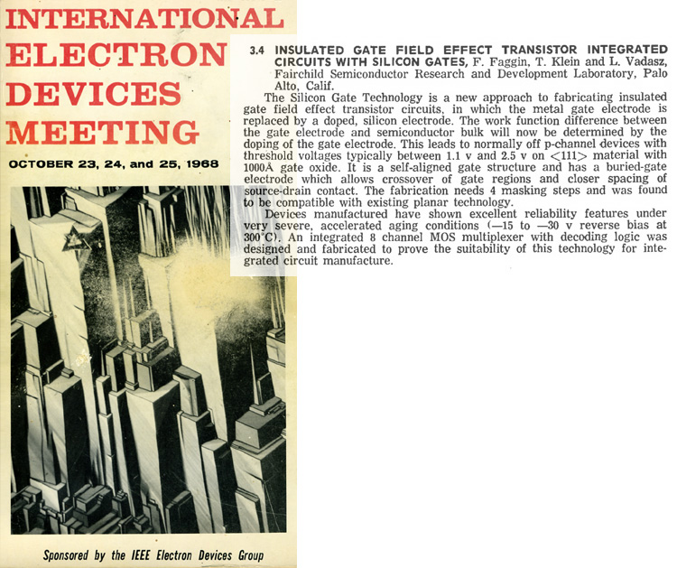
Faggin, F., Klein, T., and Vadasz, L.: Insulated Gate Field Effect Transistor Integrated Circuits with Silicon Gates.Cover and abstract of the IEDM (International Electron Devices Meeting) Program (October 1968). The Silicon Gate Technology (SGT), created at Fairchild Semiconductor in 1968, was first presented by its co-inventor and developer, Federico Faggin, at the IEDM on October 23, 1968, in Washington, D.C. It was the only commercial process technology for the fabrication of MOS integrated circuits with self-aligned gate that was later universally adopted by the semiconductor industry. The SGT was the first technology to produce commercial dynamic RAMs, CCD image sensors, non volatile memories and the microprocessor, providing for the first time all the fundamental elements of a general purpose computer with LSI integrated circuits.
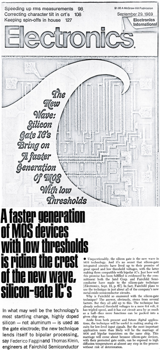
Federico Faggin and Thomas Klein.: "A Faster Generation of MOS Devices with Low Thresholds is Riding the Crest of the New Wave, Silicon-Gate IC's".Cover of Electronics Magazine (29 September 1969). The Electronics article introduces the Fairchild 3708, designed by Federico Faggin in 1968. It was the world's first commercial integrated circuit using the Silicon Gate Technology, proving its viability, and it was the first application of the new technology.
F. Faggin, T. Klein: Silicon-Gate Technology. "Solid State Electronics", 1970, Vo. 13, pp.1125–1144
Earliest documents on the Intel 4004
Initials F.F. (Federico Faggin) on the 4004 design (1971). The 4004 bears the initials F.F. of its designer, Federico Faggin, etched on one corner of the chip. Signing the chip was a spontaneous gesture of proud authorship and was also an original idea imitated after him by many Intel designers.
F. Faggin and M. E. Hoff: "Standard parts and custom design merge in four-chip processor kit". Electronics/April 24, 1972, pp.112–116. Reprinted on pp.6–27 to 6–31 of The Intel Memory Design Handbook: August 1973.
F. Faggin, M. Shima, M. E. Hoff Jr., H. Feeney, S. Mazor: "The MCS-4—An LSI micro computer system". IEEE '72 Region Six Conference. Reprinted on pp.6–32 to 6–37 of The Intel Memory Design Handbook: August 1973.
Busicom 141-PF Printing Calculator Engineering Prototype (1971). (Gift of Federico Faggin to the Computer History Museum, Mountain View, CA). The CHM collection catalog shows pictures of the engineering prototype of the Busicom 141-PF desktop calculator. The engineering prototype used the world's first microprocessor to have ever been produced. This one-of-a-kind prototype was a personal present by Busicom's president Mr. Yoshio Kojima to Federico Faggin for his successful leadership of the design and development of the 4004 and three other memory and I/O chips (the MCS-4 chipset). After keeping it in his home for 25 years, Faggin donated it to the CHM in 1996.
Faggin, F.; Capocaccia, F. "A New Integrated MOS Shift Register", Proceedings XV International Electronics Scientific Congress, Rome, April 1968, pp.143–152. This paper describes a novel static MOS shift register, developed at SGS-Fairchild (now ST Micro) at the end of 1967, before Federico Faggin joined Fairchild's R&D in Palo Alto (Ca) in February 1968. Faggin later used this new shift register in the MCS-4 chips, including the 4004(1970).
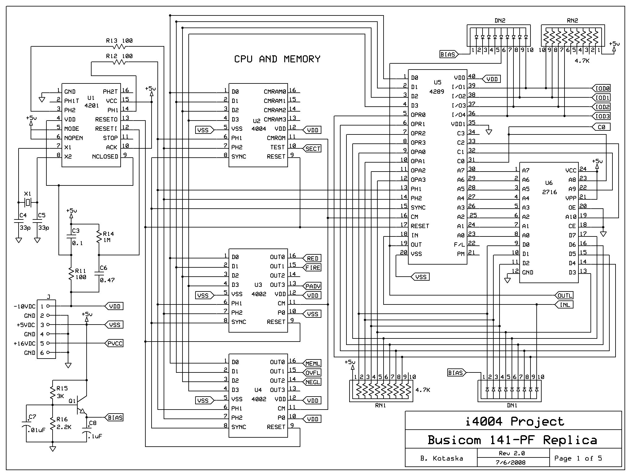
Intel 4004 -- 45th Anniversary Project, Schematics at the unofficial 4004 website, and a simulator in Java. Fully functional 130x scale replicas of the 4004 built using discrete transistors.
This page is based on this Wikipedia article Text is available under the CC BY-SA 4.0 license; additional terms may apply. Images, videos and audio are available under their respective licenses.


